

Thin-layer chemical transistor and making method
a chemical transistor and thin-layer technology, applied in the field of shottky barrier gate field-effect transistors, can solve the problems of imposing a certain limit to the desire to reduce the tft manufacturing cost, unable to avoid the introduction of small defects in the formation of tfts, and the tendency to increase the probability of tft manufacturing defects, so as to achieve the effect of minimizing defects
- Summary
- Abstract
- Description
- Claims
- Application Information
AI Technical Summary
Benefits of technology
Problems solved by technology
Method used
Image

Examples
example 1
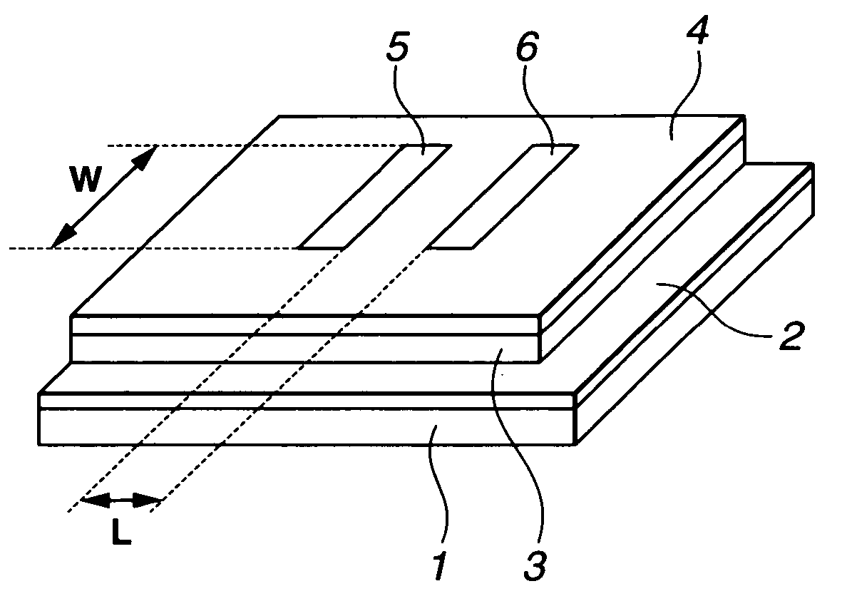
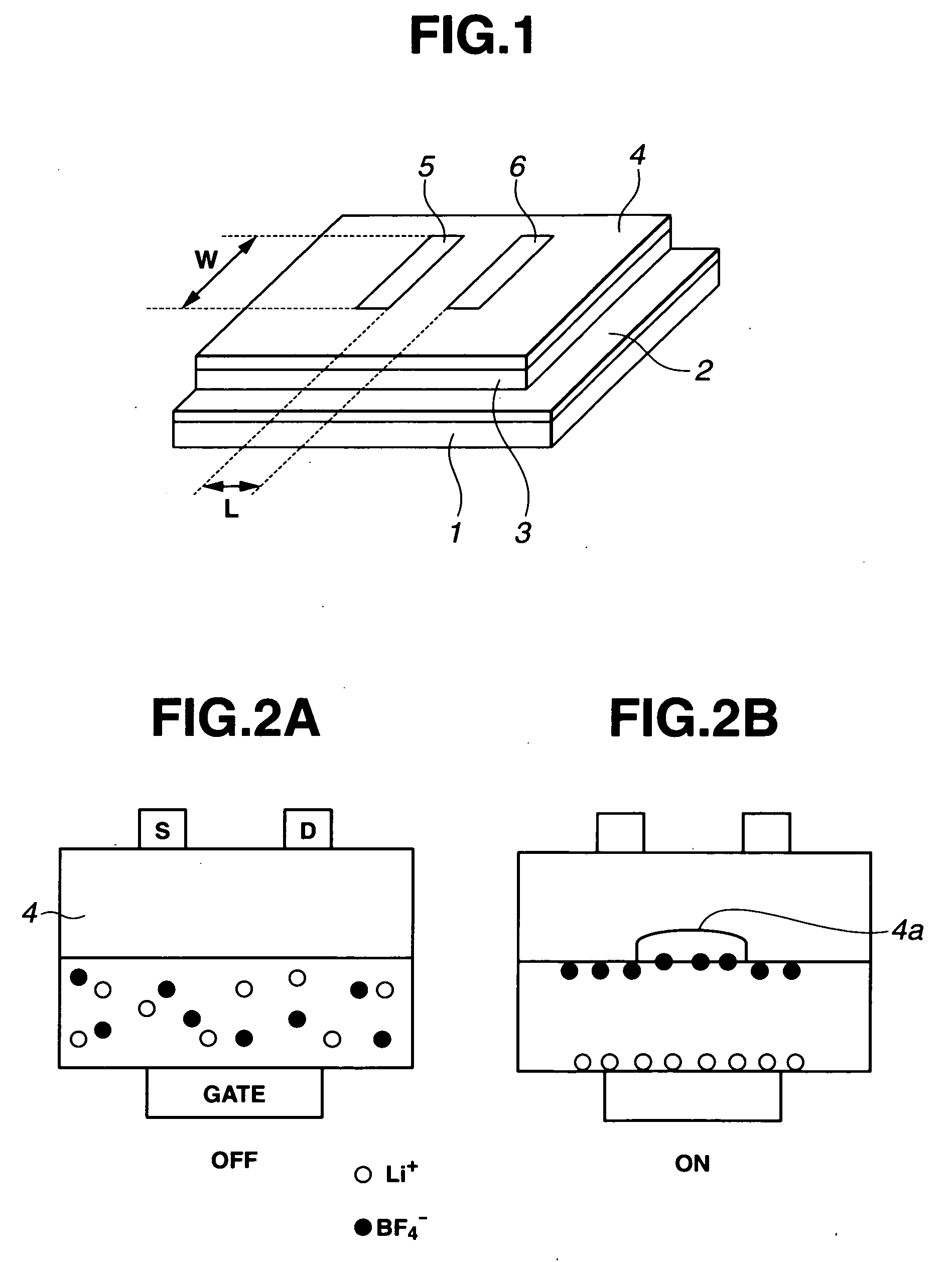
[0042] The polymer for forming the solid electrolyte layer was cyanoethylpullulan having a degree of substitution with cyanotheyl groups of 85.2 mol % (CyEPL, by Shin-Etsu Chemical Co., Ltd., CR-S, Mw: 49,000, bis-2-cyanoethyl ether content: 46 ppm). The inorganic ion salt used was LiBF4. The material for forming the semiconductor layer was poly(3-hexylthiophene) (P3HT, Aldrich, Mw: 87,000). The organic solvent for dissolving poly(3-hexylthiophene) (P3HT) was chloroform in which the cyanoethylpullulan was not dissolvable. Using these materials, a thin-layer chemical transistor was fabricated by the following procedure. It was then tested.
[0043] A gate electrode was formed on a glass (SiO2) substrate by vapor depositing Ti to a thickness of 5 nm and then Au to a thickness of 20 nm, both by RF sputtering at room temperature and a back pressure of 10−4 Pa.
[0044] Cyanoethylpullulan was dissolved in N-methyl-2-pyrrolidone in a concentration of 15 wt %. To the solution, LiBF4 was added ...
PUM
| Property | Measurement | Unit |
|---|---|---|
| dielectric constant | aaaaa | aaaaa |
| dielectric constant | aaaaa | aaaaa |
| thickness | aaaaa | aaaaa |
Abstract
Description
Claims
Application Information