Film formation apparatus and method of using the same

a technology of film formation apparatus and film, which is applied in the direction of cleaning using liquids, instruments, and final product manufacturing, etc., can solve the problems of reducing the yield of semiconductor devices being fabricated, and conventional cleaning methods of this kind have some difficulty in cleaning

Inactive Publication Date: 2006-03-02
TOKYO ELECTRON LTD +1
View PDF6 Cites 65 Cited by
  • Summary
  • Abstract
  • Description
  • Claims
  • Application Information

AI Technical Summary

Benefits of technology

[0010] An object of the present invention is to provide a film formation apparatus for a semiconductor process and a method of using the same, which allow cleaning to be performed for an optimum cleaning time period.

Problems solved by technology

The particles may drop on the semiconductor wafer, which reduces the yield of semiconductor devices being fabricated.
However, as described later, the present inventors have found that conventional cleaning methods of this kind have some difficulty in performing cleaning for an optimum cleaning time period (which varies depending on the conditions inside a reaction tube).

Method used


Image

  • Film formation apparatus and method of using the same
  • Film formation apparatus and method of using the same
  • Film formation apparatus and method of using the same

Examples


example 1

PRESENT EXAMPLE 1

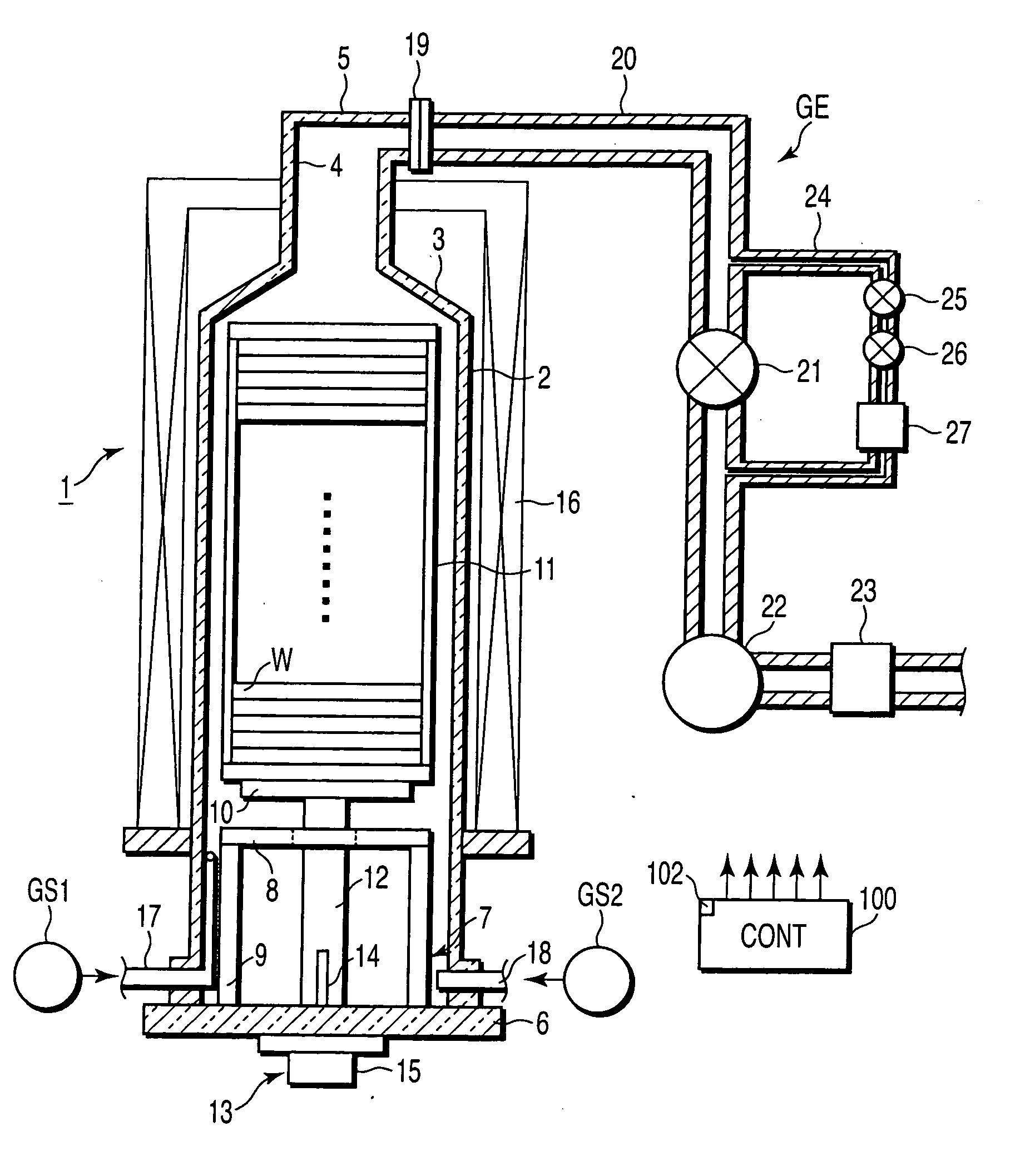
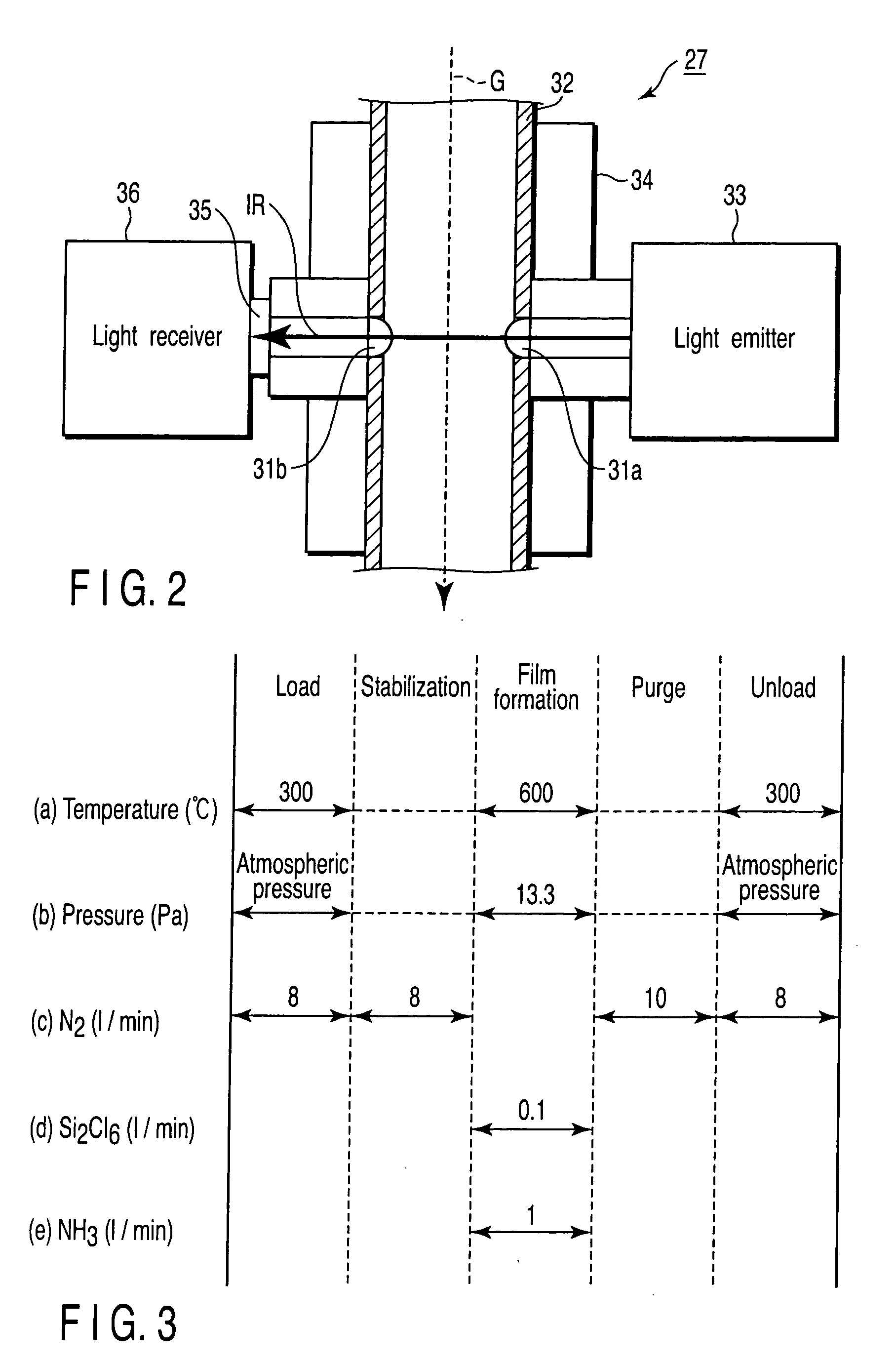
[0085] In a present example 1, using the apparatus shown in FIG. 1, a silicon nitride film of 5 μm was deposited on the inner wall of the reaction tube 2, and a cleaning process was performed thereon, under conditions described with reference to the recipe shown in FIG. 4. At this time, the concentration of silicon tetrafluoride contained in cleaning exhaust gas was monitored by the infrared sensor 27.

[0086]FIG. 5 is a graph showing change with time in the concentration of silicon tetrafluoride contained in cleaning exhaust gas, obtained by this experiment. As shown in FIG. 5, the concentration of silicon tetrafluoride increased essentially simultaneously with the start of cleaning (2 minutes in the time scale of FIG. 5), and, at about 45 minutes later (47 minutes in the time scale of FIG. 5), it returned to the same level as that of before cleaning. In this case, 45 minutes after the start of cleaning can be regarded as the end point of cleaning.

[0087] In the pre...


PUM

PropertyMeasurementUnit
temperatureaaaaaaaaaa
flow rateaaaaaaaaaa

Abstract

A film formation apparatus for a semiconductor process includes a cleaning gas supply circuit, a concentration measuring section, and an information processor. The cleaning gas supply circuit is configured to supply a cleaning gas into a reaction chamber to perform cleaning of removing from an inner surface of the reaction chamber a by-product film derived from a film formation gas. The concentration measuring section is disposed in an exhaust system to monitor concentration of a predetermined component contained in exhaust gas from the reaction chamber. The information processor is configured to compare a measurement value obtained by the concentration measuring section with a preset value and to thereby determine an end point of the cleaning.

Description

CROSS-REFERENCE TO RELATED APPLICATIONS [0001] This application is based upon and claims the benefit of priority from prior Japanese Patent Application No. 2004-245749, filed Aug. 25, 2004, the entire contents of which are incorporated herein by reference. BACKGROUND OF THE INVENTION [0002] 1. Field of the Invention [0003] The present invention relates to a film formation apparatus for a semiconductor process for forming a film on a target substrate, such as a semiconductor wafer, and also to a method of using the apparatus. The term “semiconductor process” used herein includes various kinds of processes which are performed to manufacture a semiconductor device or a structure having wiring layers, electrodes, and the like to be connected to a semiconductor device, on a target substrate, such as a semiconductor wafer or a glass substrate used for an LCD (Liquid Crystal Display) or FPD (Flat Panel Display), by forming semiconductor layers, insulating layers, and conductive layers in p...

Claims


Application Information

Patent Timeline
Patent Type & Authority Applications(United States)
IPC IPC(8): B08B3/12C23C16/00
CPCC23C16/4405Y02C20/30C23C16/4412Y02P70/50
Inventor HASEBE, KAZUHIDENODERA, NOBUTAKEENDO, ATSUSHIUMEKI, MAKOTONISHIMURA, KATSUMIMINAMI, MASAKAZUYOSHIDA, MAKOTO
Owner TOKYO ELECTRON LTD
Why Eureka
Try Eureka