
Semiconductor memory apparatus

a memory apparatus and semiconductor technology, applied in the direction of digital storage, instrumentation, water treatment parameter control, etc., can solve the problems of large time consumption, large voltage difference between bit-line pairs, and increased operation timing of inputting and outputting data, so as to prevent errors and optimally discharge.

Active Publication Date: 2009-12-03
SK HYNIX INC
View PDF14 Cites 2 Cited by
  • Summary
  • Abstract
  • Description
  • Claims
  • Application Information

AI Technical Summary

Benefits of technology

This approach prevents errors and stabilizes the bit-line sense amplifier operations by controlling the discharge period of the overdriving voltage, maintaining optimal voltage levels and reducing operational timing.

Problems solved by technology

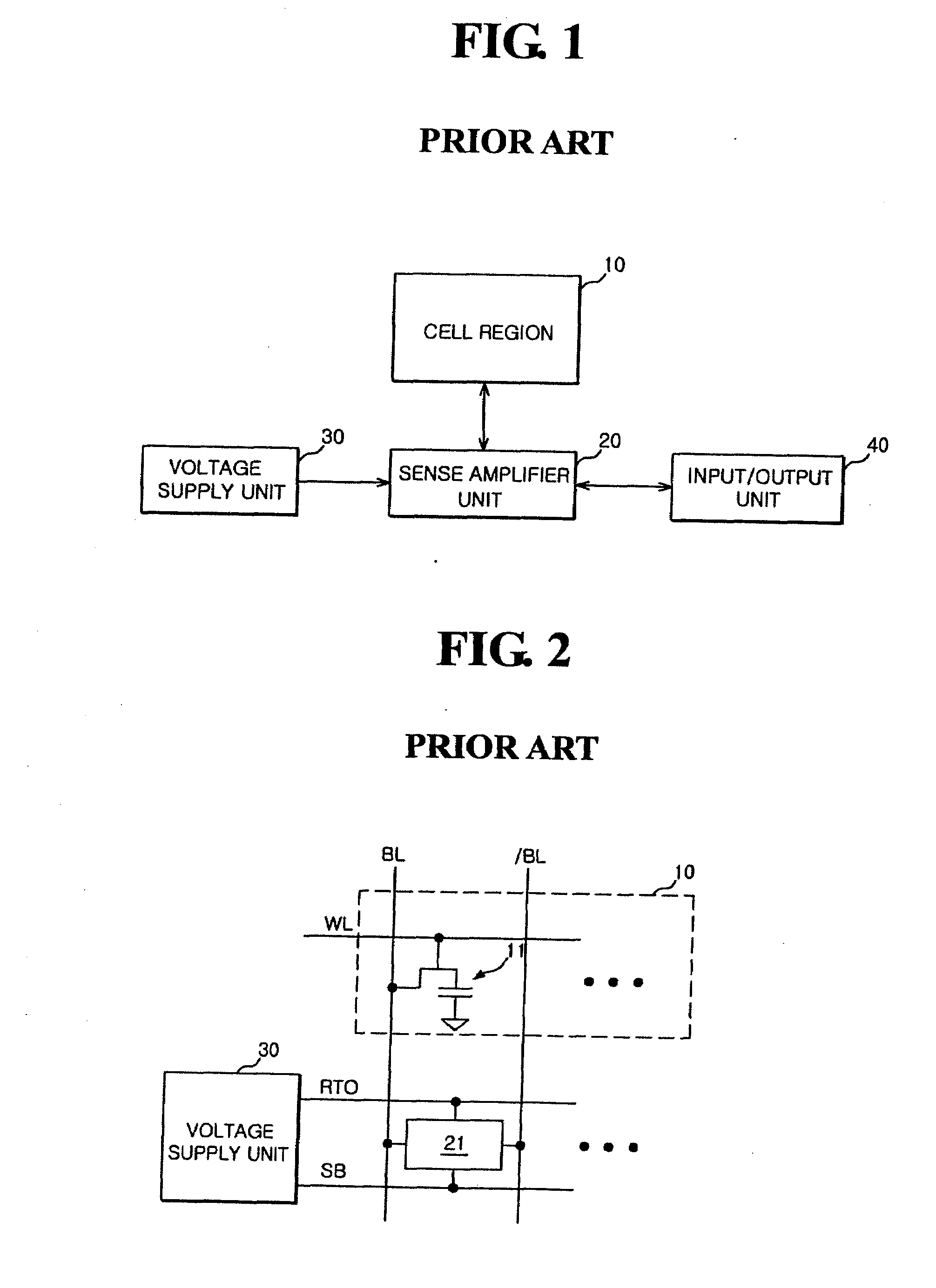
However, even though the power consumption is reduced due to the reduced potential of the power supply voltage of the semiconductor memory apparatus, there is a problem in that an operational timing for inputting and outputting data is increased.
That is, there is a problem in that the voltage difference between the bit-line pair is reduced due to the decreased level of power supply voltage, and thus it takes a large amount of time to detect and amplify the voltage difference.
However, the level of the power supply voltage or the core voltage of the semiconductor memory apparatus may be varied due to noise.
Also, when the level of the power supply voltage and the core voltage are changed depending on a type of the applied system, the detecting process or the amplifying process of the bit-line sense amplifier may not be smoothly performed due to the operation that discharges the elevated level of the bit-line sense amplifier driving voltage RTO during the selective timing.
Further, when the level of the bit-line sense amplifier driving voltage RTO is significantly over discharged, an error may occur in the following operating of the bit-line sense amplifier after the over driving operation.

Method used


Image

  • Semiconductor memory apparatus
  • Semiconductor memory apparatus
  • Semiconductor memory apparatus

Examples


Embodiment Construction

[0043]Hereinafter, preferred embodiments of the present invention will be described below in detail with reference to the accompanying drawings.

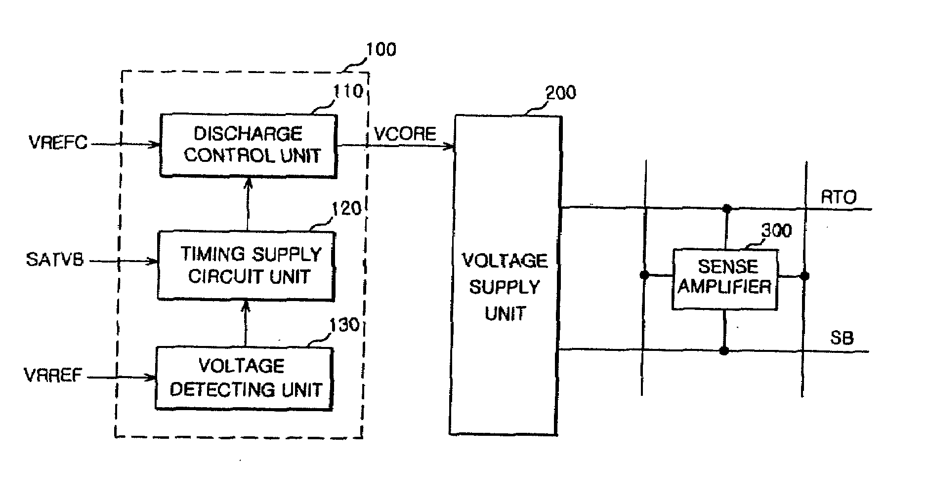
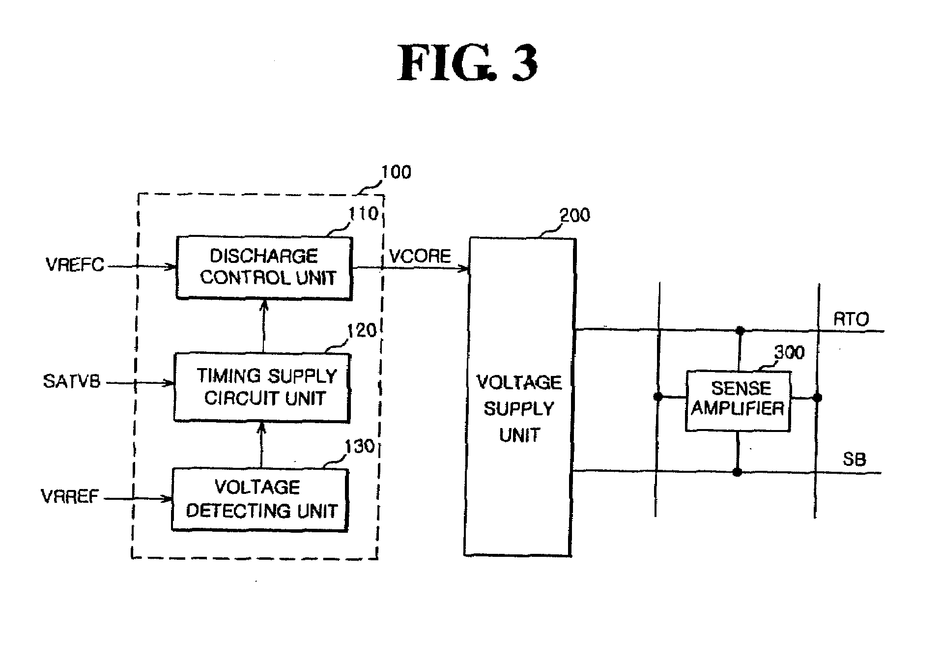
[0044]Referring to FIG. 3, a semiconductor memory apparatus according to the embodiment includes a sense amplifier 300 that has two input lines, receives a driving voltage through a sense amplifier power supply input terminal RTO and detects and amplifies a difference between signals that are supplied to the two input lines.

[0045]The semiconductor memory apparatus further includes a sense amplifier voltage supply unit 200 that supplies a driving voltage and an overdriving voltage to the sense amplifier 300 through the sense amplifier power supply input terminal RTO using a power supply voltage. The overdriving voltage is higher than the driving voltage.

[0046]The semiconductor memory apparatus further includes a driving voltage control unit 100. The driving voltage control unit 100 maintains a driving voltage level of the sense amplifier powe...


PUM


Abstract

A semiconductor memory apparatus includes a sense amplifier that receives a driving voltage through a sense amplifier power supply input terminal and detects and amplifies a difference between signals that are supplied to two input lines, a sense amplifier voltage supply unit that supplies a driving voltage and an overdriving voltage higher than the driving voltage to the sense amplifier through the sense amplifier power supply input terminal using a power supply voltage, and a driving voltage control unit that maintains a driving voltage level of the sense amplifier power supply input terminal in response to the level of the power supply voltage, after a voltage of the sense amplifier power supply input terminal is elevated to a power supply level responding to the overdriving voltage in order to perform the overdriving operation.

Description

CROSS-REFERENCE TO RELATED PATENT APPLICATION[0001]This application is a divisional of U.S. patent application Ser. No. 11 / 637,758, filed Dec. 13, 2006, the subject matter of which application is incorporated herein by reference in its entirety.[0002]This application claims the benefit of Korean Patent Application No. 10-2006-0019444, filed on Feb. 28, 2006, in the Korean Intellectual Property Office, the disclosure of which is incorporated herein in its entirety by reference.BACKGROUND OF THE INVENTION[0003]1. Technical Field[0004]The present invention relates to a semiconductor memory apparatus, and in particular, to a power supply circuit for a bit-line sense amplifier of a semiconductor memory apparatus.[0005]2. Related Art[0006]As semiconductor related technologies are developed, the number of memory cells in semiconductor memory apparatuses increases. Therefore, when manufacturing semiconductor memory apparatuses, by making a unit cell that is capable of storing data have the ...

Claims


Application Information

Patent Timeline
Patent Type & Authority Applications(United States)
IPC IPC(8): G11C7/02G11C7/00
CPCG11C7/065G11C2207/065G11C7/08C02F11/122C02F2209/03
Inventor CHO, HO YOUB
Owner SK HYNIX INC
Learn More