

Semiconductor device having super junction structure and method for manufacturing the same
a technology of super junction structure and semiconductor device, which is applied in the direction of semiconductor device, basic electric element, electrical apparatus, etc., can solve the problems of limited withstand voltage reduction, achieve the effect of improving the withstand voltage of the device having the sj structure, improving the yield ratio of products, and easy manufacturing of the sj structur
- Summary
- Abstract
- Description
- Claims
- Application Information
AI Technical Summary
Benefits of technology
Problems solved by technology
Method used
Image

Examples
first embodiment
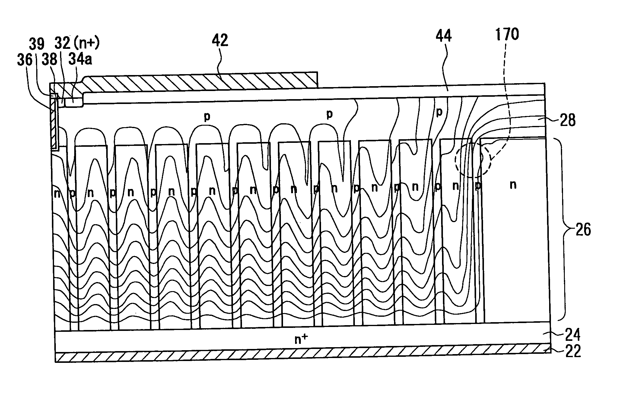
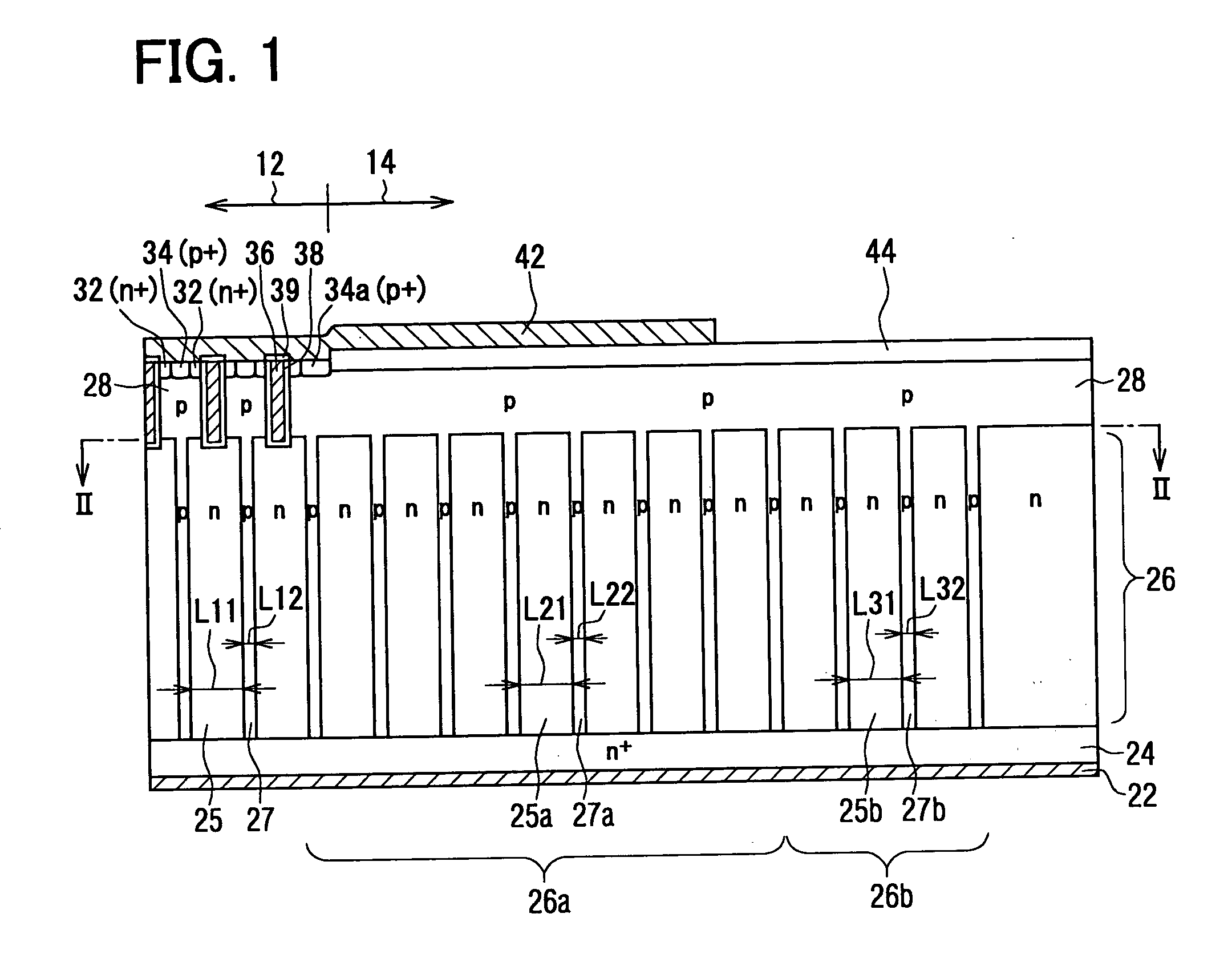
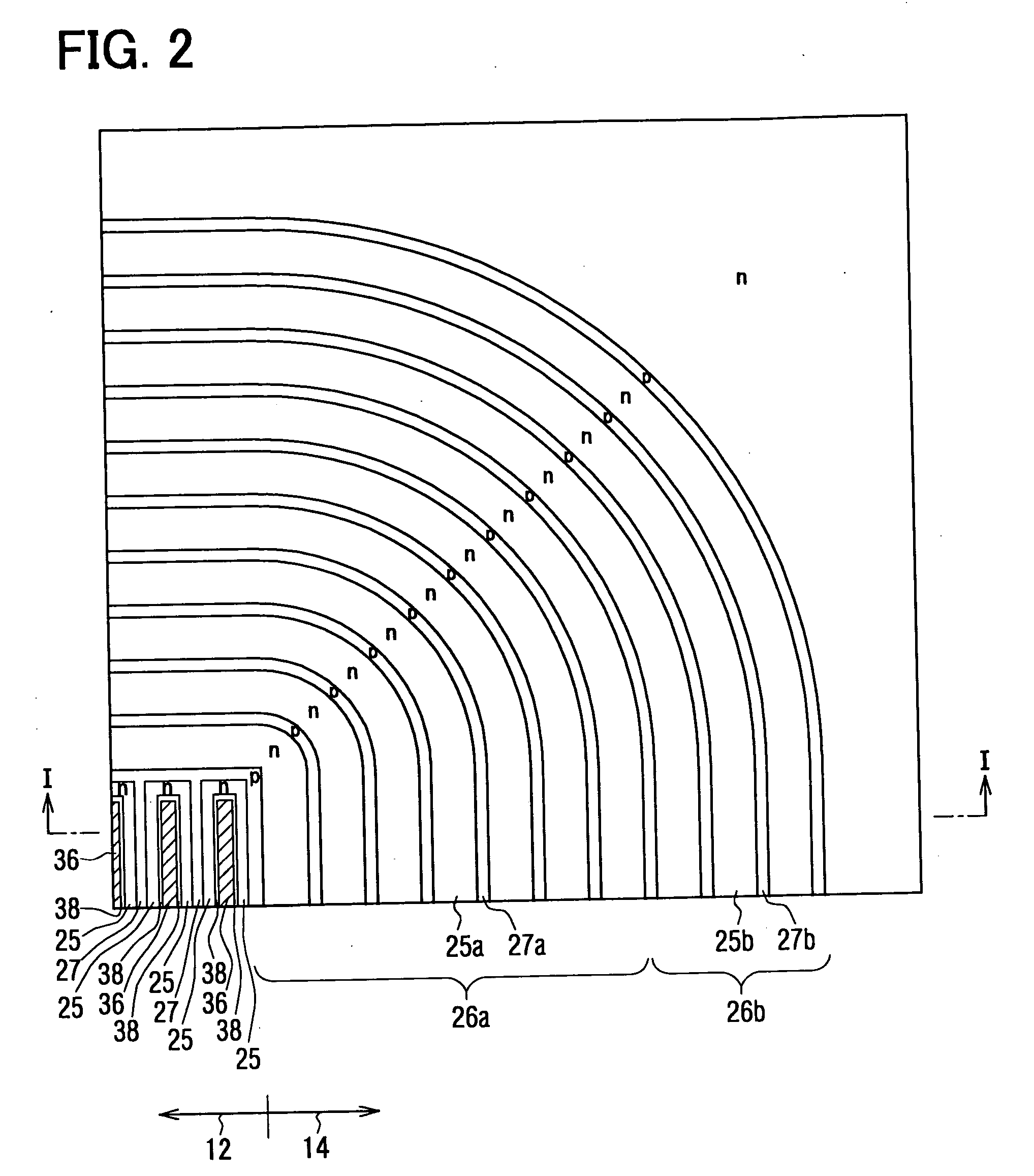
[0027] A semiconductor device having a super junction (i.e., SJ) structure according to a first embodiment of the present invention is shown in FIGS. 1 and 2. FIG. 1 is a partial cross sectional view showing a center region 12 and a periphery region 14 of the device. FIG. 2 is a partial plan view showing the device corresponding to line II-II in FIG. 1. Here, FIG. 1 shows the device taken along line I-I in FIG. 2. Specifically, FIG. 2 shows a main part of the device represents, specifically, a corner of the device.
[0028] The device is mainly made of silicon-based semiconductor. However, the device can be made of another semiconductor material.
[0029] As shown in FIG. 1, the center region 12 includes a semiconductor switching device, and the periphery region 14 is disposed around the center region 12. In this device, the switching device is formed of a MOSFET. Specifically, the device includes a N+ conductive type (i.e., N+) drain layer 24, a drift layer 26 as an example of a semico...
second embodiment
[0057] A semiconductor device having a SJ structure according to a second embodiment of the present invention is shown in FIG. 12.
[0058] The N columns 25 and the P columns 27 in the center region 12 are repeated alternately in a horizontal direction. The N columns 25a, 25b and the P columns 27a, 27b in the inner and the outer periphery regions 26a, 26b are also repeated alternately in the same horizontal direction. The periphery region 14 includes three parts which are composed of the inner and the outer periphery regions 26a, 26b and the third periphery region 26c. The third periphery region 26c includes the N column 25c and the P column 27c, which are formed to extend from the N column 25 and the P column in the center region 12. Thus, the width of the N column 25c in the third periphery region 26c is equal to the width of the N column 25 in the center region 12. Further, the width of the P column 27c in the third periphery region 26c is equal to the width of the P column 27 in t...
PUM
 Abstract
Description
Claims
Application Information