Method and apparatus for magnetization test of write head in a disk drive
- Summary
- Abstract
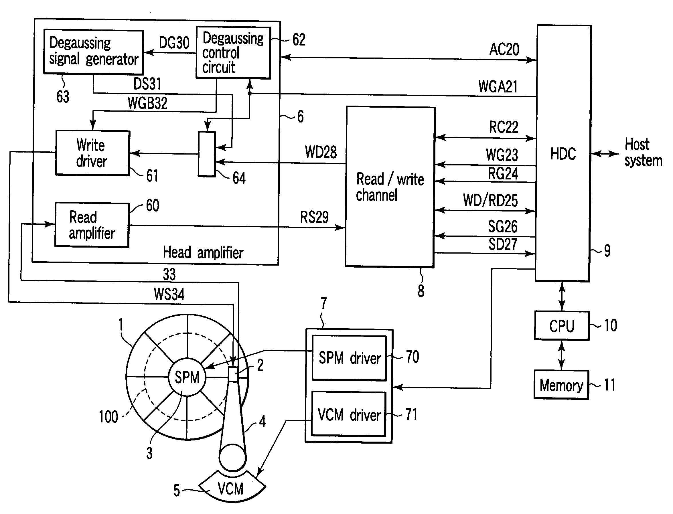
- Description
- Claims
- Application Information
AI Technical Summary
Benefits of technology
Problems solved by technology
Method used
Image

Examples
second embodiment
[0070]FIG. 5 and FIGS. 6A to 6L illustrate the second embodiment of the present invention.
[0071] In the magnetization test mode wherein L=3, M=1, and N=1, the HDC 9 of the second embodiment performs write gate control in such a manner that P write gates WGA21 are issued between servo sectors (P: a multiple of “3”).
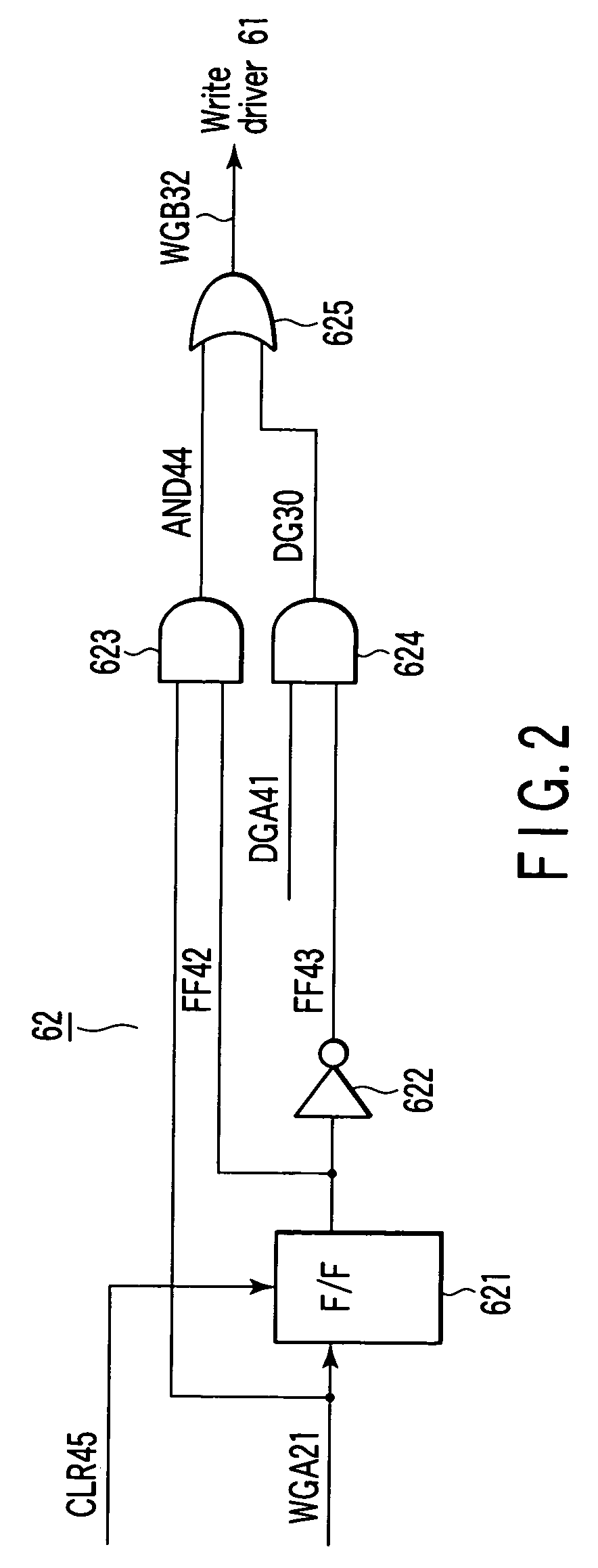
[0072] As shown in FIG. 5, the degaussing control circuit 62 of the present embodiment comprises flip-flops 621A and 621B, invertors 622, 627 and 628, AND gates 623, 624 and 626, NAND gate 629, and OR gate 625.
[0073] Referring to the timing chart shown in FIGS. 6A to 6L, a description will be given as to how the head amplifier unit 6 operates in the degaussing test mode of the disk drive. That is, a description will be given of the test write sequence.
[0074] The HDC 9 supplies a switching signal to the head amplifier unit 6 by way of signal line AC20, so as to switch to the degaussing test mode. In the degaussing control circuit 62, flip-flop 621A is initialized by CLS...
third embodiment
[0085]FIG. 7 and FIGS. 8A to 8L illustrate the third present embodiment of the present invention.
[0086] In the magnetization test mode wherein L=3, M=1, and N=1, the HDC 9 of the third embodiment performs write gate control in such a manner that P write gates WGA21 are issued between servo sectors (P: a multiple of “3”), as in the second embodiment described above.
[0087] In the description below, reference will be made mainly to the differences the third embodiment has over the second embodiment.
[0088] As shown in FIG. 7, the degaussing control circuit 62 of the present embodiment comprises flip-flops 621A and 621B, invertors 622, 627 and 628, AND gates 623, 624 and 626, NAND gate 629, and OR gate 625. The degaussing control circuit 62 shown in FIG. 7 differs from that shown in FIG. 5 in the configuration of ANDE gate circuit 623.
[0089] The HDC 9 outputs write gate WGA21 and write data WD28 (see FIGS. 8B and 8C). The degaussing control circuit 62 switches off the gate control si...
PUM
 Abstract
Description
Claims
Application Information
 - R&D
- Intellectual Property
- Life Sciences
- Materials
- Tech Scout
- Unparalleled Data Quality
- Higher Quality Content
- 60% Fewer Hallucinations
Browse by: Latest US Patents, China's latest patents, Technical Efficacy Thesaurus, Application Domain, Technology Topic, Popular Technical Reports.
© 2025 PatSnap. All rights reserved.Legal|Privacy policy|Modern Slavery Act Transparency Statement|Sitemap|About US| Contact US: help@patsnap.com