MTJ elements with high spin polarization layers configured for spin-transfer switching and spintronics devices using the magnetic elements

a technology of high spin polarization layer and magnetic element, which is applied in the manufacture of inductance/transformer/magnet, magnetic body, instruments, etc., can solve the problems of affecting the utility and reliability of such conventional magnetic elements, increasing power consumption, and conventional magnetic elements b>10/b>, and achieves the effect of low write curren

Active Publication Date: 2006-06-29
SAMSUNG SEMICON
View PDF7 Cites 191 Cited by
  • Summary
  • Abstract
  • Description
  • Claims
  • Application Information

AI Technical Summary

Benefits of technology

[0013] According to the method and system disclosed herein, the present invention provides a magnetic

Problems solved by technology

Use of a high critical current for switching the magnetization 19/19′ adversely affects the utility and reliability of such conventional magnetic elements 10/10′ in a magnetic memory.
The use of a high write current is associated with increased power consumption, which is undesirable.
In addition, the conventional magnetic element 10′, which has a higher resistance and thus a higher signal

Method used


Image

  • MTJ elements with high spin polarization layers configured for spin-transfer switching and spintronics devices using the magnetic elements
  • MTJ elements with high spin polarization layers configured for spin-transfer switching and spintronics devices using the magnetic elements
  • MTJ elements with high spin polarization layers configured for spin-transfer switching and spintronics devices using the magnetic elements

Examples


first embodiment

[0031]FIG. 3 is a diagram of a magnetic element 100 in accordance with the present invention and which can be written using spin transfer. The magnetic element 100 includes a first pinning layer 102 that is preferably an AFM layer, first pinned layer 104, a first barrier layer 112, a free layer 114, a second barrier layer 116, a second pinned layer 118, and a second pinning layer 120. Also depicted are capping layer(s) 122. In an alternate embodiment, the first pinning layer 102 and / or the second pinning layer 120 may be omitted in favor of another mechanism for pinning the magnetizations of the pinned layers 104 and 118. In a preferred embodiment, the AFM layers 102 and 120 include materials such as PtMn and IrMn. In addition, seed layers 103 may be used on the substrate 101 to provide a desired texture of the AFM layer 102. Any ferromagnetic layers, such as the free layer 114, first pinned layer 104 (or ferromagnetic layers 106 and 110), and the second pinned layer 118 include at ...

second embodiment

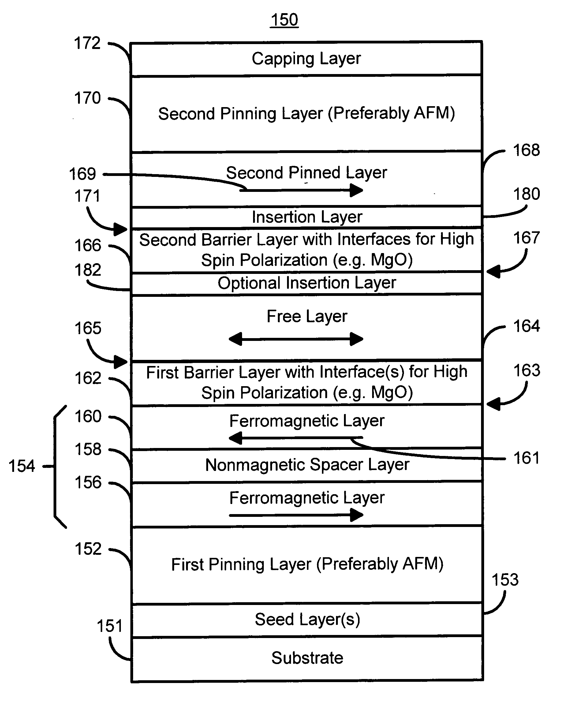
[0041]FIG. 5 is a diagram of a magnetic element 150 in accordance with the present invention and which can be written using spin transfer. The magnetic element 150 includes a first pinning layer 152 that is preferably an AFM layer, first pinned layer 154, a first barrier layer 162, a free layer 164, a second barrier layer 166, a second pinned layer 168, and a second pinning layer 170. Also depicted are capping layer(s) 172. In an alternate embodiment, the first pinning layer 152 and / or the second pinning layer 170 may be omitted in favor of another mechanism for pinning the magnetizations of the pinned layers 154 and 168. In a preferred embodiment, the AFM layers 152 and 170 include materials such as PtMn and IrMn. In addition, seed layers 153 may be used on the substrate 151 to provide a desired texture of the AFM layer 152. Any ferromagnetic layers, such as the free layer 164, first pinned layer 154 (or ferromagnetic layers 156 and 160), and the second pinned layer 168 include at ...

third embodiment

[0051]FIG. 8 is a diagram of a magnetic element 200 in accordance with the present invention and which can be written using spin transfer. The magnetic element 200 includes a pinning layer 202 that is preferably an AFM layer, pinned layer 204, a barrier layer 212, and a free layer 214. Also depicted are capping layer(s) 216. In an alternate embodiment, the pinning layer 202 may be omitted in favor of another mechanism for pinning the magnetizations of the pinned layer 204. In a preferred embodiment, the AFM layer 202 includes materials such as PtMn and IrMn. In addition, seed layers 203 may be used on the substrate 201 to provide a desired texture of the AFM layer 202. Any ferromagnetic layers, such as the free layer 214 and pinned layer 204 (or ferromagnetic layers 206 and 210) include at least one of Ni, Co, and Fe. For example, such materials include but are not limited to CoFe, CoFe, Ni, CoFeB (with B being at least five and no more than thirty atomic percent), CoFeC, and CoFeHf...


PUM


Abstract

A method and system for providing a magnetic element are disclosed. The method and system include providing first and second pinned layers, a free layer, and first and second barrier layers between the first and second pinned layers, respectively, and the free layer. The first barrier layer is preferably crystalline MgO, which is insulating, and configured to allow tunneling through the first barrier layer. Furthermore, the first barrier layer has an interface with another layer, such as the free layer or the first pinned layer. The interface has a structure that provides a high spin polarization of at least fifty percent and preferably over eighty percent. The second barrier layer is insulating and configured to allow tunneling through the second barrier layer. The magnetic element is configured to allow the free layer to be switched due to spin transfer when a write current is passed through the magnetic element.

Description

FIELD OF THE INVENTION [0001] The present invention relates to magnetic memory systems, and more particularly to a method and system for providing a magnetic element having an improved signal and that can be switched using a spin transfer effect at a lower switching current. BACKGROUND OF THE INVENTION [0002]FIGS. 1A and 1B depict conventional magnetic elements 10 and 10′. Such conventional magnetic elements 10 / 10′ can be used in non-volatile memories, such as magnetic random access memories (MRAM). The conventional magnetic element 10 is a spin valve and includes a conventional antiferromagnetic (AFM) layer 12, a conventional pinned layer 14, a conventional nonmagnetic spacer layer 16 and a conventional free layer 18. Other layers (not shown), such as seed or capping layer may also be used. The conventional pinned layer 14 and the conventional free layer 18 are ferromagnetic. Thus, the conventional free layer 18 is depicted as having a changeable magnetization 19. The conventional ...

Claims


Application Information

Patent Timeline
IPC IPC(8): H01L21/00H01L29/94G11C11/22
CPCB82Y25/00B82Y40/00G11C11/16H01F10/3204H01F10/3254H01F10/3286H01F10/3272H01F10/3281H01F41/302H01L43/08H01F10/3263H10N50/10H10B61/00
Inventor HUAI, YIMINGPAKALA, MAHENDRA
Owner SAMSUNG SEMICON
Why Eureka
Try Eureka