Integrated semiconductor circuit and method for producing an integrated semiconductor circuit

Inactive Publication Date: 2006-03-09
INFINEON TECH AG
View PDF9 Cites 15 Cited by
  • Summary
  • Abstract
  • Description
  • Claims
  • Application Information

AI Technical Summary

Benefits of technology

[0011] One advantage of the present invention consists in the fact that, independently of one another, the contact terminal provided for testing can be optimized with regard to its mechanical stability and the contact terminal provided for the subsequent permanent contact connection can be optimized with regard to a minimum capacitance with respect to the substrate. In particular, the contact terminal provided for the permanent contact connection in the case of flip-chip mounting has, relative to its area, a lower electrostatic capacitance with respect to the substrate than the contact provided for the testing of the semiconductor circuit.
[0012] Furthermore, the two contact terminals can also be optimized independently of one another with regard to their lateral extent or their area, so that both the contact terminal provided for the temporary contact connection by a probe of a probe card and the contact terminal provided for a permanent contact connection in the case of flip-chip mounting have the required minimum area in each case.
[0013] If the area required for the contact connection by a probe of a probe card is significantly smaller than the area required for the permanent contact connectio

Problems solved by technology

The magnitude of the electrostatic capacitance of each input and output of an integrated semiconductor circuit may limit performance in this case since the capacitance results in a low-impedance property at

Method used


Image

  • Integrated semiconductor circuit and method for producing an integrated semiconductor circuit
  • Integrated semiconductor circuit and method for producing an integrated semiconductor circuit
  • Integrated semiconductor circuit and method for producing an integrated semiconductor circuit

Examples


Example

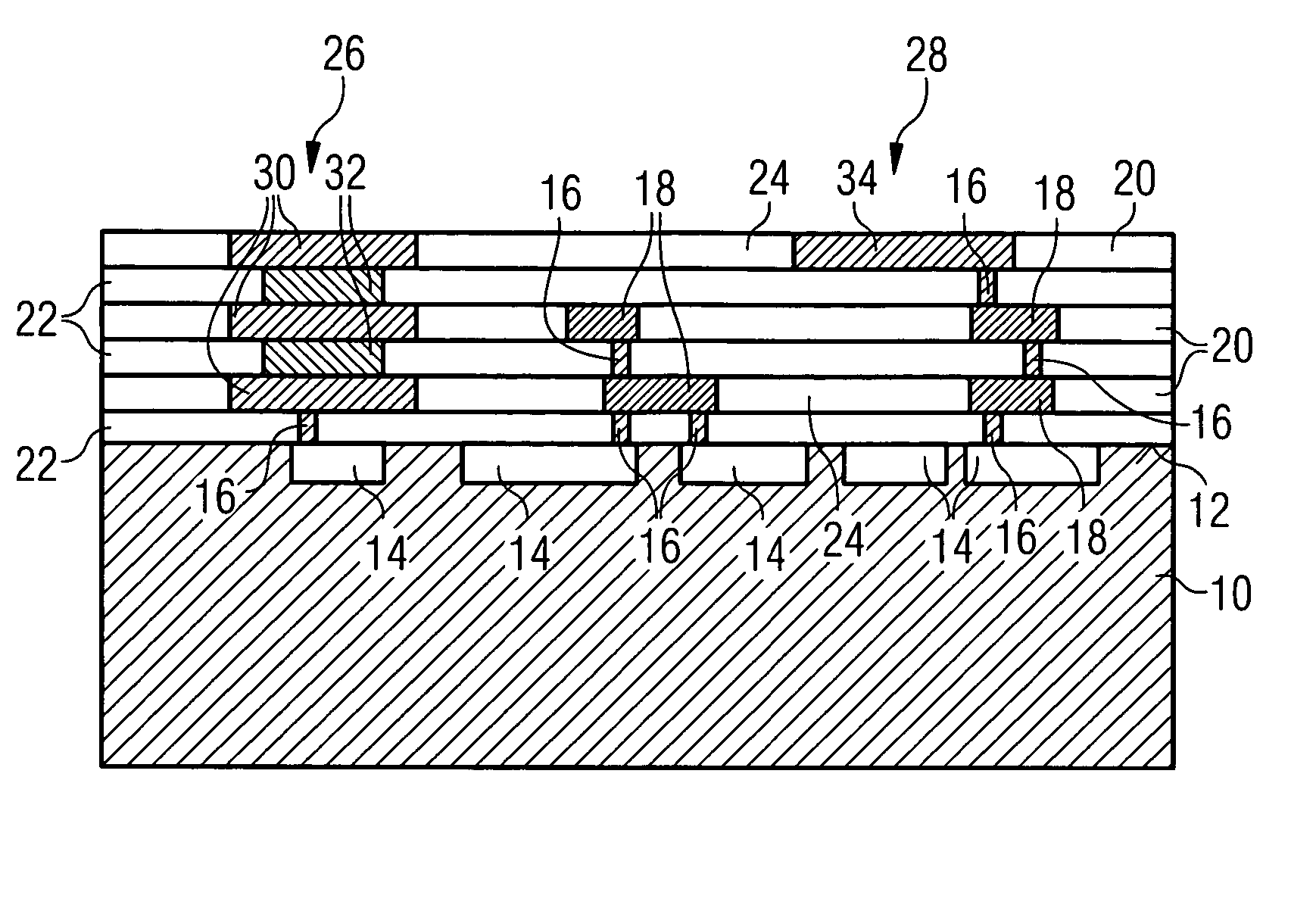
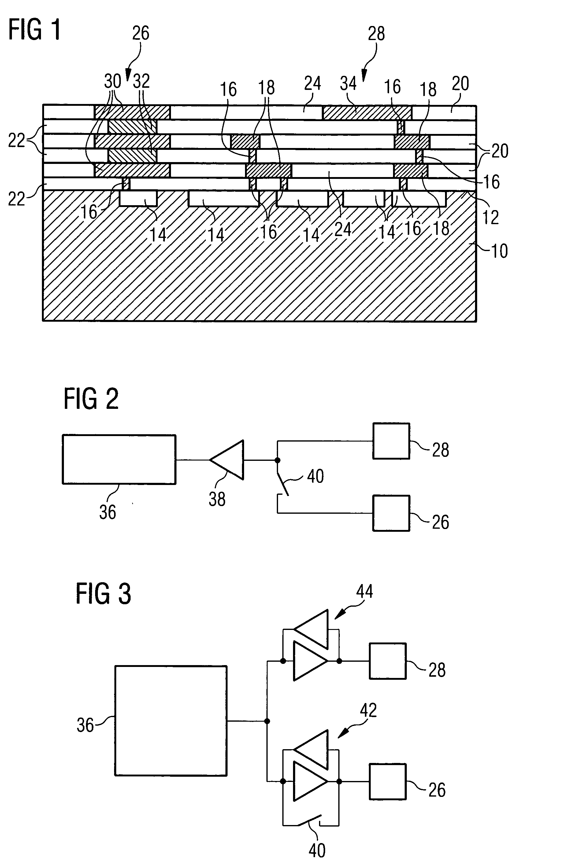
[0020]FIG. 1 is a schematic illustration of a vertical section through an integrated semiconductor circuit in accordance with one embodiment of the present invention. In a substrate 10, electronic components 14 are arranged at the surface 12 thereof. The components 14 may be transistors, diodes, capacitors, resistors or other components. If the integrated semiconductor circuit is a memory circuit, for example a DRAM memory circuit, the components 14 may be memory cells, input and output amplifiers or drivers, row and column decoders, and other circuits or subcircuits of the memory circuit. For this purpose, the components 14 are interconnected or connected to one another via through-hole conductors 16 and interconnects 18.

[0021] The interconnects 18 are arranged in a plurality of wiring planes 20 that are isolated from one another and from the substrate 10 or the surface 12 thereof in each case by an insulator layer 22. Interconnects 18 and other conductive structures—described bel...


PUM


Abstract

An integrated semiconductor circuit comprises a substrate with a circuit, a plurality of wiring planes that are isolated from one another and from the substrate by insulator layers, and a signal path for the circuit in the substrate and/or the wiring planes. A first contact terminal, which is formed from a stack of metal areas in a plurality of the wiring planes, is designed for connecting the signal path to an external signal source or an external signal receiver during a test of the integrated semiconductor circuit. A second contact terminal, which is formed from a metal area or from a stack of metal areas in a plurality of wiring planes, is designed for connecting the signal path to an external signal source or an external signal receiver during normal operation of the integrated semiconductor circuit. The distance between the metal area or the bottommost metal area of the stack of the second contact terminal and the substrate is greater than the distance between the bottommost metal area of the stack of the first contact terminal and the substrate.

Description

CROSS-REFERENCE TO RELATED APPLICATIONS [0001] This application claims foreign priority benefits under 35 U.S.C. §119 to co-pending German patent application number DE 10 2004 041 961.2, filed 31 Aug. 2004. This related patent application is herein incorporated by reference in its entirety. BACKGROUND OF THE INVENTION [0002] 1. Field of the Invention [0003] The present invention relates to an integrated semiconductor circuit, including an integrated semiconductor circuit with a low electrostatic capacitance between a contact terminal and a substrate, and to a method for producing the semiconductor circuit. [0004] 2. Description of the Related Art [0005] An important trend in practically all integrated semiconductor circuits, for example DRAM and other memory components, is toward ever faster data exchange. The magnitude of the electrostatic capacitance of each input and output of an integrated semiconductor circuit may limit performance in this case since the capacitance results in ...

Claims


Application Information

Patent Timeline
IPC IPC(8): H01L23/12
CPCH01L24/03H01L24/05H01L2924/00014H01L2224/05599H01L2924/01013H01L2924/01027H01L2924/01078H01L2924/14H01L2924/19041H01L2924/19043H01L2924/30105H01L2924/3011H01L2924/01006H01L2924/01033H01L2924/01068
Inventor SCHAEFER, ANDRE
Owner INFINEON TECH AG
Why Eureka
Try Eureka