Transflective liquid crystal display device

Inactive Publication Date: 2006-03-09
SHARP KK
View PDF11 Cites 40 Cited by
  • Summary
  • Abstract
  • Description
  • Claims
  • Application Information

AI Technical Summary

Benefits of technology

[0030] In the present invention, the first thin film transistor is connected to the reflective electrode and the second thin film transistor is connected to the transparent electrode. Accordingly, it is possible to supply individual data signals respectively to the reflective electrode and the transparent electrode by controlling the first and second thin film transistors, and therefore reflectance-applied voltage characteristic (R-V characteristic) in the reflective region can be substantially matched to transmittance-applied voltage characterist

Problems solved by technology

Accordingly, there arises difference between the lights passing through the transmissive region and the reflective region as to the variances in the polarizing direction, and therefore the amount of light emitted upward from the panel unfavorably differs between the regions even if the same amount of lights enter the transmissive region and the reflective region.
For this reason, even when a voltage applied is appropriately set for the device to exhibit an excellent display performance when the device is used as a transmissive liquid crystal display device, for example, excellent display cannot be achieved if the liquid crystal display device is used as a reflective liquid crystal display device.
However, there

Method used


Image

  • Transflective liquid crystal display device
  • Transflective liquid crystal display device
  • Transflective liquid crystal display device

Examples


first embodiment

[0045]FIG. 4 is a perspective view showing the configuration of a transflective liquid crystal display device of a first embodiment of the present invention. FIG. 5 is a block diagram showing the circuit configuration of the same transflective liquid crystal display device. Note that, in this embodiment, a description will be given of an example in which the present invention is applied to a VA mode transflective liquid crystal display device.

[0046] As shown in FIG. 4, the transflective liquid crystal display device of this embodiment includes a liquid crystal panel 105, a drive circuit board 106 connected to the liquid crystal panel 105, a backlight unit 107 placed on one surface side of the liquid crystal panel 105 (under the liquid crystal panel 105 in FIG. 4), and a pair of circularly polarizing plates (not shown) placed to sandwich the liquid crystal panel 105.

[0047] As shown in FIG. 5, a drive circuit which drives the liquid crystal panel 105 includes a control unit 100, a v...

second embodiment

[0082]FIG. 11 is a plan view showing a transflective liquid crystal display device of a second embodiment of the present invention. In FIG. 11, the same components as in FIG. 6 are denoted by the same numerals, and the detailed description thereof will be omitted.

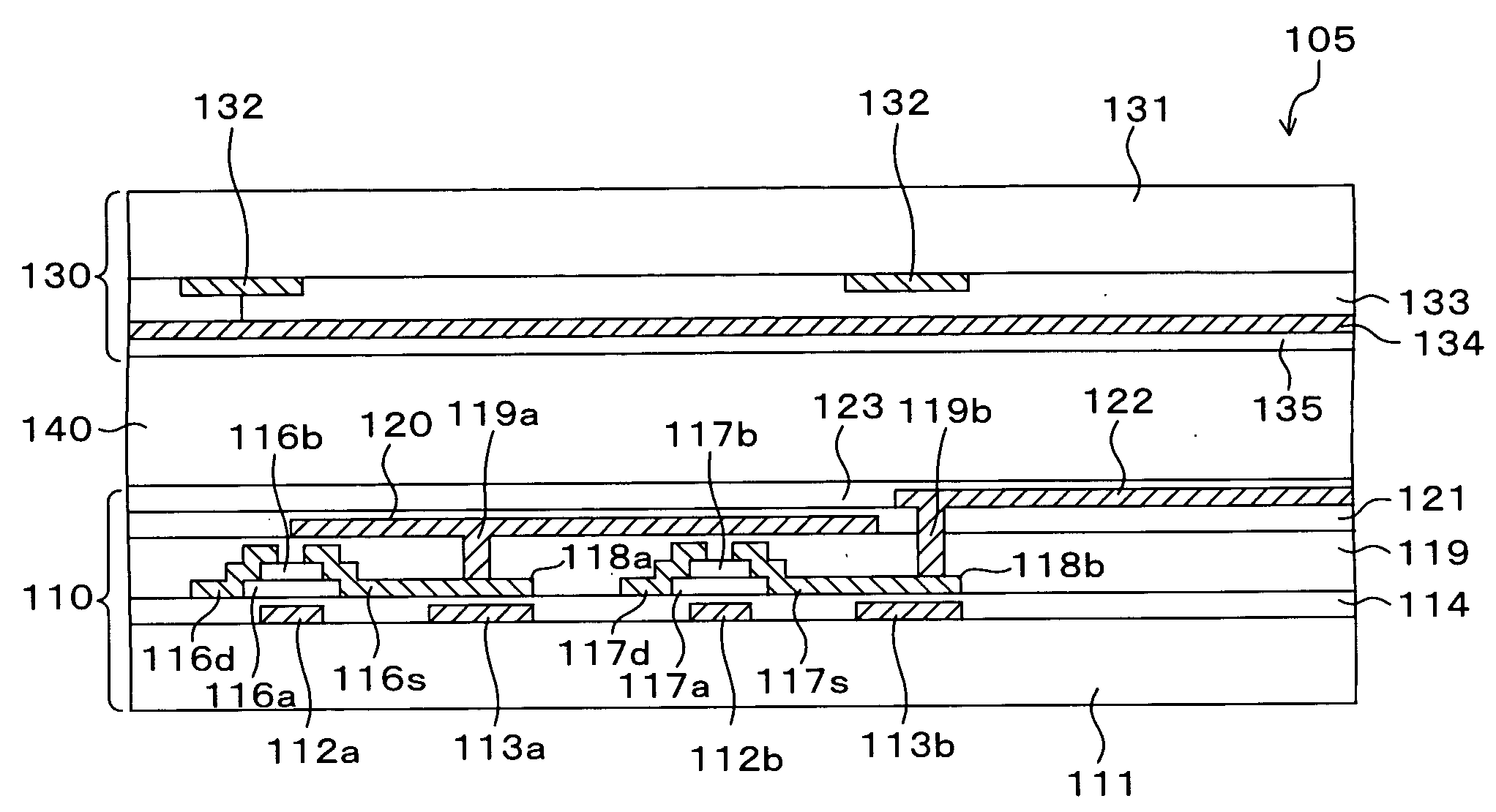
[0083] In this embodiment, the source electrode 116s of the first TFT 116 is electrically connected to a transparent electrode 203 via a contact hole 202a. The first auxiliary capacitor bus line 113a and a first auxiliary capacitor electrode 201a are placed below the transparent electrode 203. The first auxiliary capacitor electrode 201a is electrically connected to the transparent electrode 203 via a contact hole 202b. The source electrode 117s of the second TFT 117 is connected to a second auxiliary capacitor electrode 201b. The second auxiliary capacitor electrode 201b is electrically connected to a reflective electrode 204 via a contact hole 202c. All of the TFT 117, the second gate bus line 112b, the second auxiliary ...

third embodiment

[0085]FIG. 12 is a block diagram showing the configuration of a transflective liquid crystal display device of a third embodiment of the present invention. In FIG. 12, the same components as in FIG. 5 are denoted by the same numerals, and the detailed description thereof will be omitted.

[0086] In the first embodiment shown in FIG. 5, gate signals to be supplied to the first and second gate bus lines 112a and 112b are generated in such a manner that the signals outputted from the data driver 103 are switched to each other by the data signal selection switches GSW. In this case, however, the gate signal selection switches GSW are required and general-purpose gate drivers cannot be used.

[0087] Accordingly, as shown in FIG. 12, two general-purpose gate drivers 211a and 211b are used, and these general-purpose gate drivers 211a and 211b are driven by use of timing signals C3 and C4, which are synchronized with each other. In this way, during one horizontal synchronization period, the g...


PUM


Abstract

A reflective electrode, a transparent electrode, a TFT connected to the reflective electrode and a TFT connected to the transparent electrode are formed in each picture element. A first data signal is written into the reflective electrode via the TFT, a second data signal is written into the transparent electrode via the TFT. In this way, the individual data signals are respectively written into the reflective electrode and the transparent electrode, and thereby excellent display quality can be obtained either when used as a transmissive liquid crystal display device or when used as a reflective liquid crystal display device.

Description

CROSS-REFERENCE TO RELATED APPLICATIONS [0001] This application is based on and claims priority of Japanese Patent Application No.2004-262713 filed on Sep. 9, 2004, the entire contents of which are incorporated herein by reference. BACKGROUND OF THE INVENTION [0002] 1. Field of the Invention [0003] The present invention relates to a transflective liquid crystal display device for displaying images by use of a backlight under dark conditions and by use of reflection of external light under well-lit conditions. [0004] 2. Description of the Prior Art [0005] Liquid crystal display devices are advantageous in that they are thin and light, as well as have low power consumption characteristics owing to its low-voltage drive capability, and are therefore widely used in various electronic devices. In particular, active matrix liquid crystal display devices including thin film transistors (TFTs) provided in respective picture elements as switching elements also exhibit excellent display quali...

Claims


Application Information

Patent Timeline
IPC IPC(8): G02F1/1335
CPCG02F1/133555G02F2001/134345G02F1/1393G02F1/13624G02F1/134345G02F1/1335
Inventor ENOMOTO, HIROMIOKAZAKI, SUSUMU
Owner SHARP KK
Why Eureka
Try Eureka