Switching element

a technology of switching elements and organic charge-transfer complexes, applied in the field of switching elements, can solve the problems of difficult to form uniform films of a large area, difficult to mass-produce switching elements using the above organic charge-transfer complexes, and the conventional organic bistable materials with two-component systems are not straightforwardly applicable to mass-production of switching elements. , to achieve the effect of excellent bistability and easy formation

Inactive Publication Date: 2006-03-16
FUJI ELECTRIC HLDG CO LTD
View PDF1 Cites 9 Cited by
  • Summary
  • Abstract
  • Description
  • Claims
  • Application Information

AI Technical Summary

Benefits of technology

[0039] Further, the above compounds of the formulas (A) to (R) are excellent in the bistability and can be easily formed into a

Problems solved by technology

However, switching elements using the above organic charge-transfer complexes have the following problems.
Particularly, when film formation is carried out by a vapor deposition method or the like, due to the difference in the vapor pressure between both components, it is difficult to form a uniform film of a large area.
Accordingly, it has been a problem that the above conventional organic bistable materials with two-component system is not straightforwardly applica

Method used


Image

  • Switching element
  • Switching element
  • Switching element

Examples


example 1

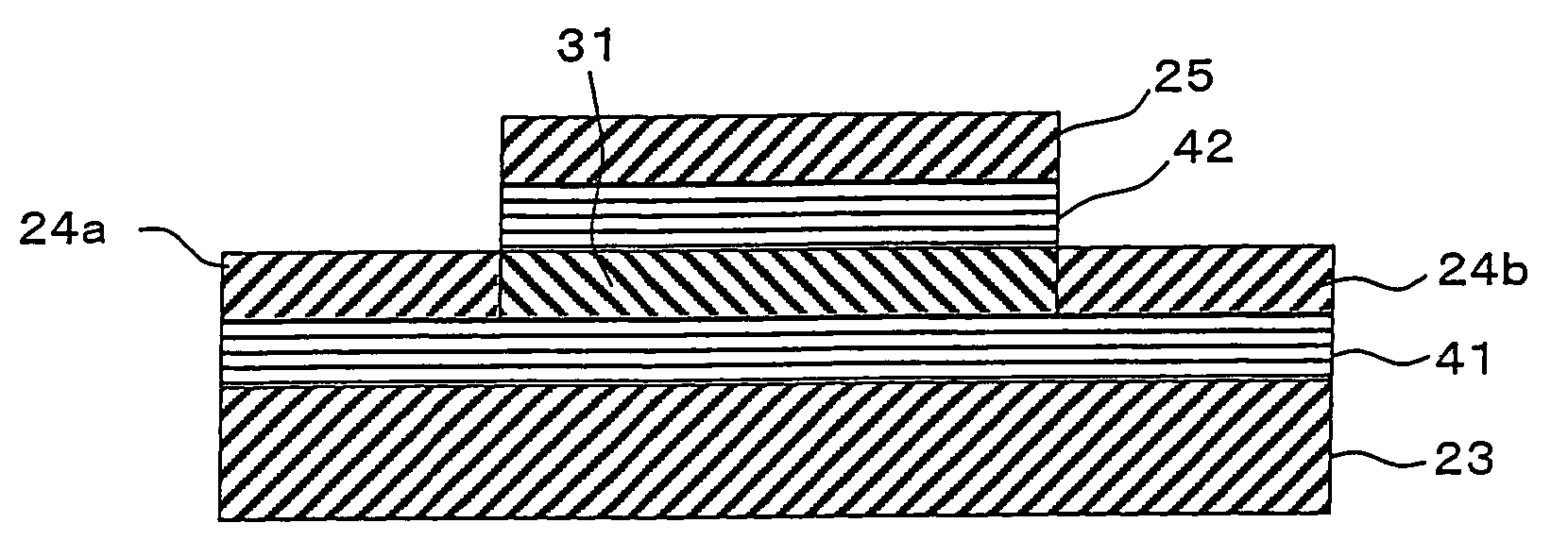
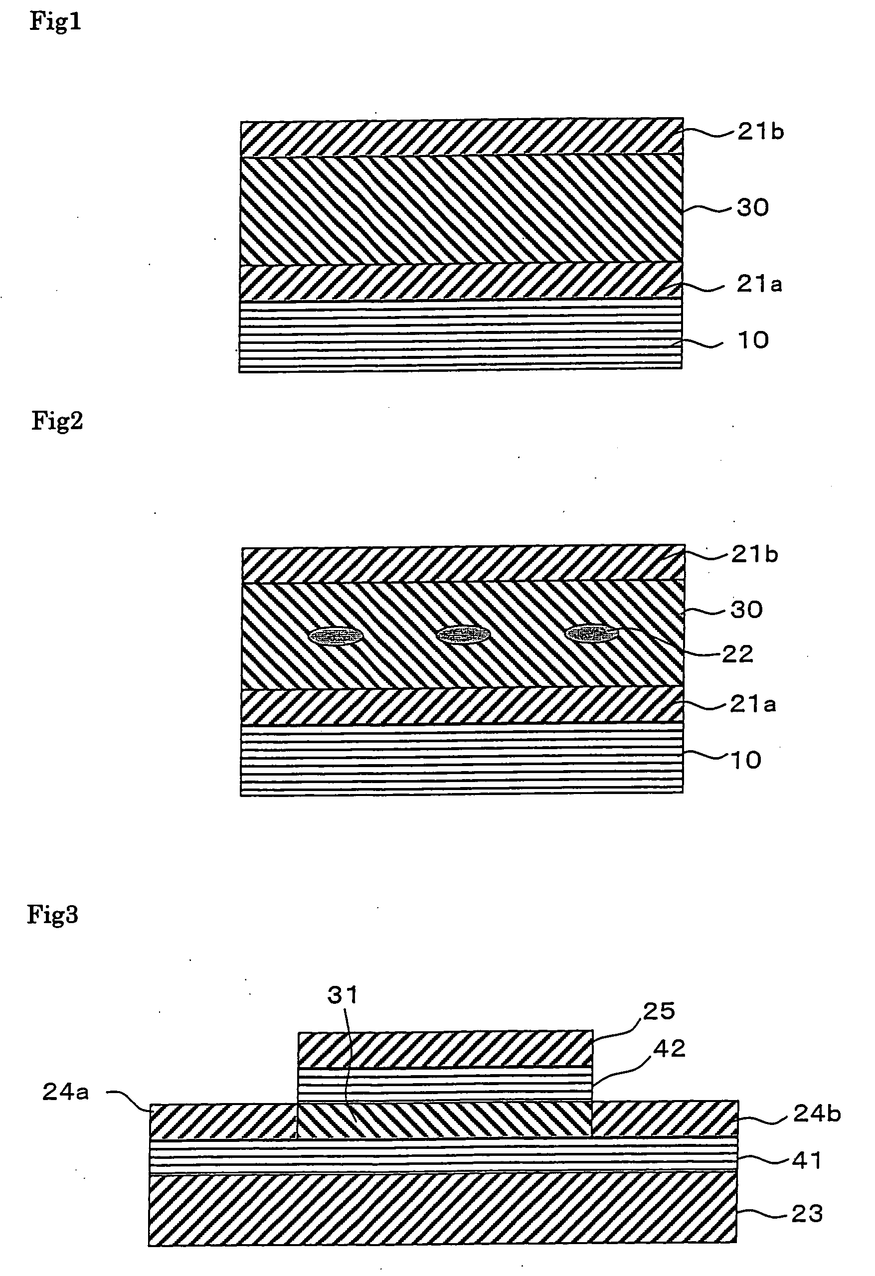
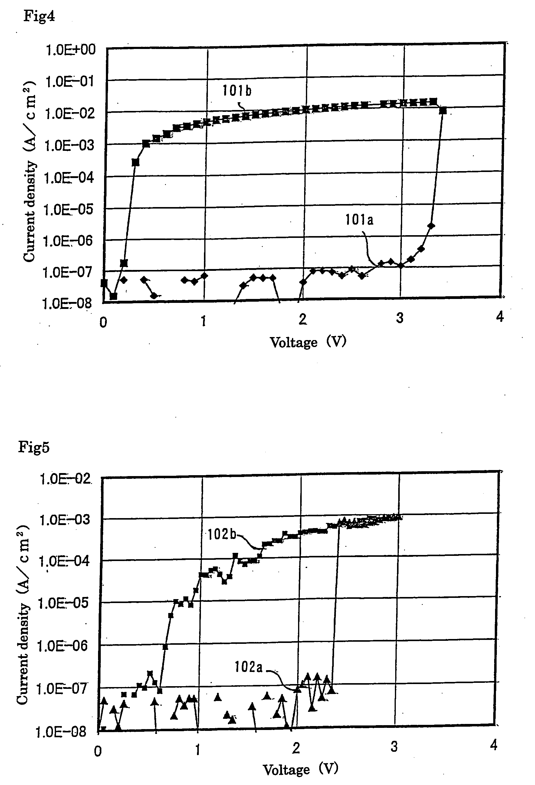
[0157] A switching element having the structure as shown in FIG. 1 was prepared by the following manner.

[0158] On a glass substrate as a substrate 10, by a vapor deposition method, thin films were successively formed in order with aluminum as an electrode layer 21a, an aminoimidazole type compound as a bistable material layer 30 and aluminum as an electrode layer 21b, to prepare a switching element of Example 1. As the aminoimidazole type compound, a compound of the following formula (A-1) was used.

[0159] Films of the electrode layer 21a, bistable material layer 30 and electrode layer 21b were formed in a thickness of 100 nm, 80 nm and 100 nm, respectively. Further, the deposition apparatus was used at a degree of vacuum of 3×10⁻⁶ torr by evacuation with a diffusion pump. The deposition of aluminum was conducted by an electrical resistance heater system at a film forming rate of 3 Å / sec, and the deposition of the aminoimidazole type compound was conducted by an electrical resista...

example 2

[0160] A switching element of Example 2 was obtained under the same conditions as in Example 1, provided that films of the electrode layer 21a, bistable material layer 30 and electrode layer 21b were formed in a thickness of 100 nm, 60 nm and 100 nm, respectively.

example 3

[0161] A switching element of Example 3 was obtained under the same conditions as in Example 1, provided that a compound of the following formula (A-2) was used as the aminoimidazole type compound, and films of the electrode layer 21a, bistable material layer 30 and electrode layer 21b were formed in a thickness of 100 nm, 60 nm and 100 nm, respectively.


PUM


Abstract

The present invention provides a switching element in which the compositional deviation of material is suppressed and that attains uniform bistability performance and is suitable for mass production. In a switching element comprising an organic bistable material, which exhibits two stable states in resistance under applied voltage, arranged between at least two electrodes, the organic bistable material comprises at least a compound having an electron-donating functional group and an electron-accepting functional group in each molecule. It is preferred that, for example, an aminoimidazole type compound, a pyridone type compound, a stilbene type compound or a butadiene type compound be used as the above compound.

Description

TECHNICAL FIELD [0001] The present invention relates to a switching element comprising an organic bistable material, the organic bistable material being arranged between two electrodes, which is utilized for a switching element driving of an organic EL display panel, a high-density memory, and the like. BACKGROUND ART [0002] In recent years, remarkable progress in characteristics of organic electronic materials has been made. Particularly, since some of low-dimensional conductors, such as charge-transfer complexes, have distinctive properties of being a material such as that with metal-insulator transition, attempts for the applications of them to a switching element driving of an organic EL display panel, a high-density memory, and the like, have been in progress. [0003] As a material applicable to a switching element, an organic bistable material is being paid attention to. The organic bistable material is an organic material that shows a so-called nonlinear response. Namely, when...

Claims


Application Information

Patent Timeline
IPC IPC(8): H01L51/00G11C13/02H01L51/05H01L51/30
CPCB82Y10/00G11C13/0014H01L27/285H01L51/0051H01L51/0052H01L51/0054H01L51/0591H01L51/006H01L51/0067H01L51/0069H01L51/0071H01L51/0072H01L51/0504H01L51/0059H10K19/202H10K85/611H10K85/615H10K85/622H10K85/631H10K85/633H10K85/654H10K85/656H10K85/657H10K85/6572H10K10/00H10K10/50
Inventor KAWAKAMI, HARUOKURODA, MASAMIKATO, HISATOSEKINE, NOBUYUKIYAMASHIRO, KEISUKEIWAMOTO, TAKUJIKOTANI, NORIKO
Owner FUJI ELECTRIC HLDG CO LTD
Why Eureka
Try Eureka