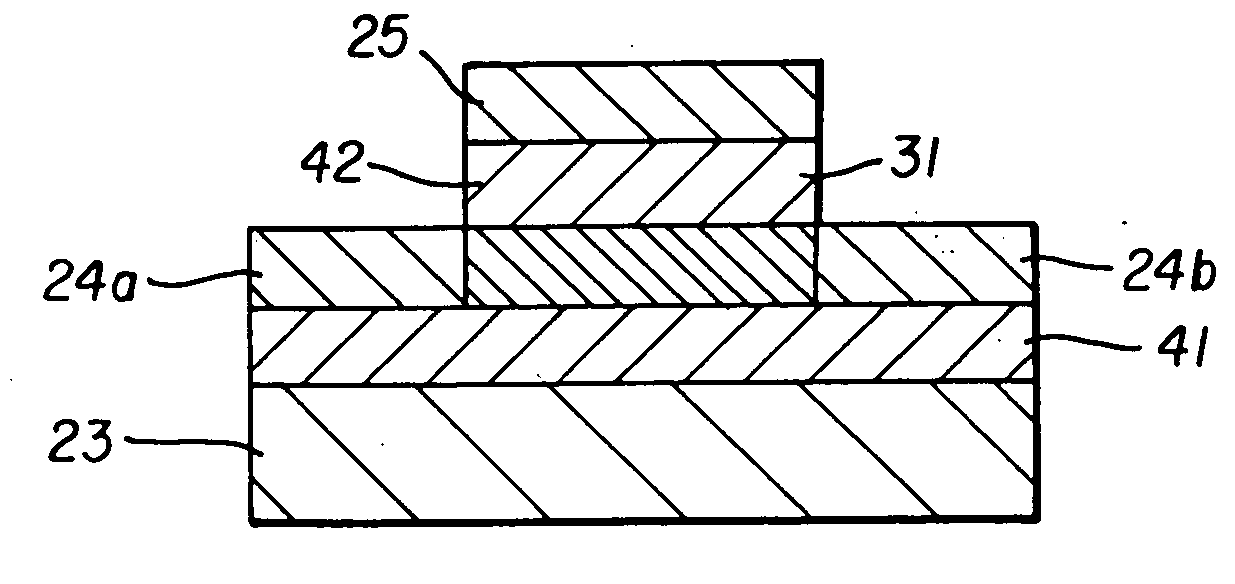
Switching element

a switching element and bistable characteristic technology, applied in thermoelectric devices, instruments, organic chemistry, etc., can solve the problems of poor cyclic performance, difficult to mass-produce a switching element having a uniform bistable characteristic and product quality, and difficult to form uniform films over a large surface area, so as to reduce the resistance of the organic bistable material layer, the effect of large electric field and good cyclic performan

Inactive Publication Date: 2007-03-22
FUJI ELECTRIC CO LTD
View PDF8 Cites 2 Cited by
  • Summary
  • Abstract
  • Description
  • Claims
  • Application Information

AI Technical Summary

Benefits of technology

[0023] With this switching element the diffused metal can be considered to behave as an acceptor. As a result, both the lowest unoccupied orbital level and the highest occupied orbital level of the diffusion zone are supposedly high. Therefore, because the diffusion zone of the metal becomes an energy barrier, a large electric field is necessary due to switching and the transition voltage apparently increases. Furthermore, because switching is not accompanied by the phase change, the cyclic performance is good.
[0024] Further, with the mode in which the above-described diffusion inhibiting layer is formed, the decrease in the resistance of the organic bistable material layer and increase in leakage current caused by excessive diffusion of the metal to the organic bistable material layer can be prevented and the leakage current can be suppressed.
[0025] In accordance with the present invention, it is preferred that the second electrode layer be formed by vapor deposition and the temperature of the substrate during the vapor deposition be 30-150° C. In this case, setting the substrate temperature during vapor deposition within this range increases the diffusion rate of the metal. Therefore, the metal constituting the second electrode layer can sufficiently diffuse into the organic bistable material layer.
[0026] Further, in accordance with the present invention, it is preferred that the second electrode layer comprise at least one species selected from gold, platinum, rhodium, silver, and chromium. The absolute value of the work function of those metals is the highest among the electrode materials and they easily behave as acceptors during diffusion into the organic bistable material. Therefore, they can be advantageously used for the present invention.

Problems solved by technology

However, the above-described switching elements using organic charge transfer complexes have the following problems.
In particular, when a film is formed by a vacuum vapor deposition method or the like, a uniform film is difficult to form over a large surface area because of the difference in vapor pressure between the two components or due to a geometric arrangement employed when separate deposition sources are used for both materials in a co-deposition method.
Therefore, in the organic bistable materials in prior arts, there is a problem that it is difficult to mass-product a switching element having a uniform bistable characteristic and product quality.
A switching element formed of organic transfer complexes, as shown in FIG. 19, has a problem that transition voltage th2 is high, about 10 V when transition is made from OFF state to the ON state, but the cyclic performance is poor.
Further, the following problem is associated with the switching element described in PCT Application No. 02 / 37500.
In particular, the transition voltage is too low in applications to a display drive such as organic EL displays.

Method used


Image

  • Switching element
  • Switching element
  • Switching element

Examples


working example 1

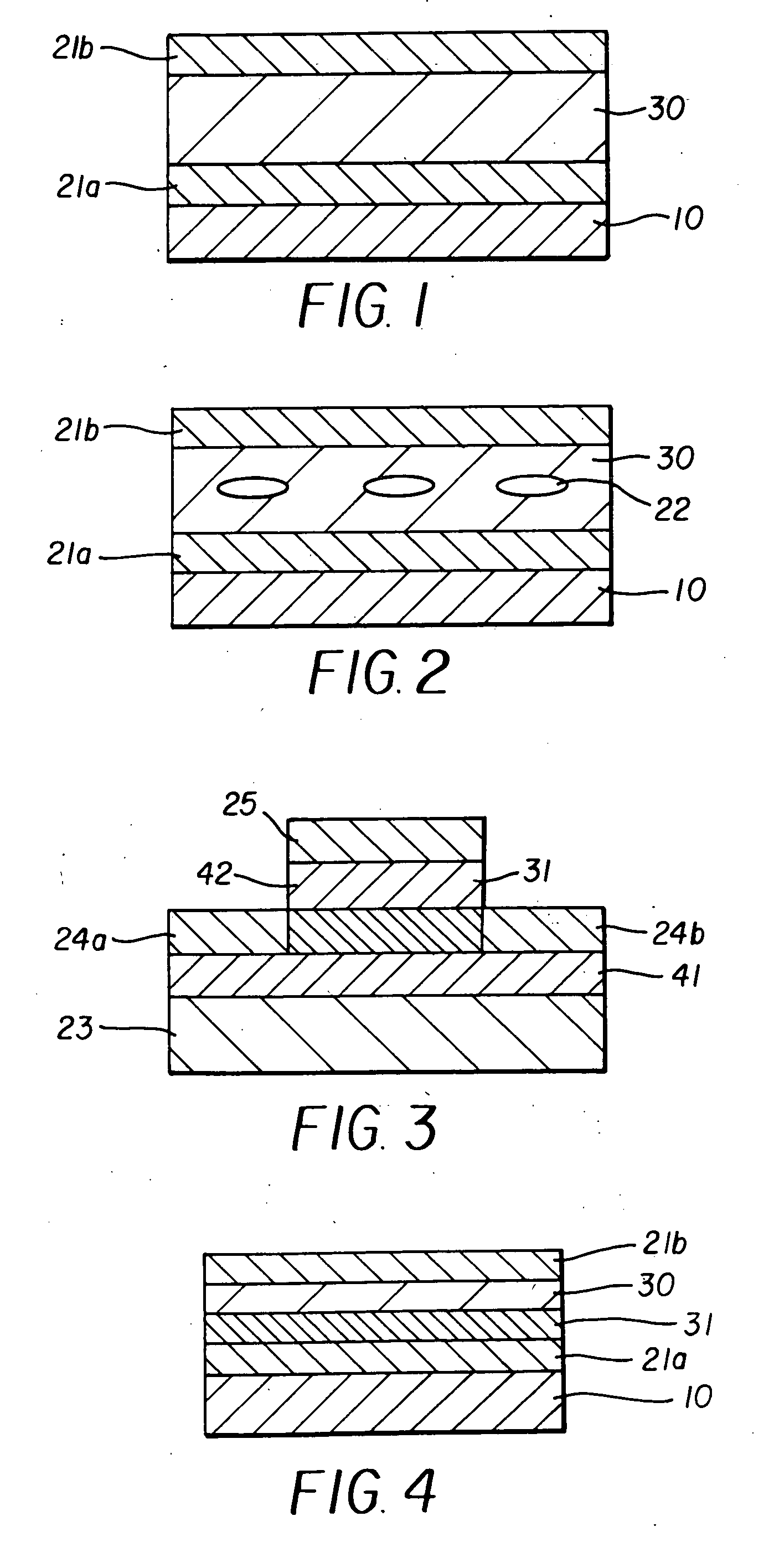
[0092] The switching element with a configuration shown in FIG. 1 was produced by the following procedure.

[0093] The switching element was formed by using a glass substrate as the substrate 10 and successively forming thin films by vacuum vapor depositing aluminum as the first electrode layer 21a, a quinomethane-based compound as the bistable material layer 30, and gold as the second electrode layer 21b. The compound with the below-described structural formula (I-1) was used as the quinomethane-based compound.

[0094] Further, the first electrode layer 21a, organic bistable material layer 30, and second electrode layer 21b were formed to have a thickness of 100 nm, 80 nm, and 100 nm, respectively. The vapor deposition apparatus performed diffusion pump gas discharge to a degree of vacuum of 3×10⁻⁶ Torr. Vapor deposition of aluminum and quinomethane-based compound was conducted at a substrate temperature of 20° C. and a film growth rate of 3 Å / sec and 2Å / sec, respectively. Further, ...

working example 2

[0095] A switching element was obtained by using the compound with the structural formula (I-13) presented below as the quinomethane-based compound and growing films under the same conditions as in Working Example 1 so that the first electrode layer 21a, organic bistable material layer 30, and second electrode layer 21b had a thickness of 100 nm, 80 nm, and 100 nm, respectively.

working example 3

[0096] In Working Example 3, a switching element was obtained under the same conditions as in Working Example 1, except that vapor deposition of aluminum, quinomethane-based compound and gold was conducted at a substrate temperature of 20° C.


PUM

PropertyMeasurementUnit
temperatureaaaaaaaaaa
transition voltage th2aaaaaaaaaa
voltageaaaaaaaaaa

Abstract

The present invention provides a switching element that has a stable bistable characteristic and a high transition voltage and demonstrates excellent cyclic performance. The switching element has two stable resistance values with respect to the voltage applied between electrodes, wherein a first electrode layer, an organic bistable material layer, and a second electrode layer are successively formed as thin films on a substrate and the organic bistable material constituting the organic bistable material layer is a quinomethane-based compound or a monoquinomethane-based compound. A metal constituting the second electrode layer is diffused into the organic bistable material layer. It is preferred that the second electrode layer be formed by vapor deposition and the temperature of the substrate during the vapor deposition be 30-150° C.

Description

TECHNICAL FIELD [0001] The present invention relates to a switching element in which an organic bistable layer is disposed between two electrodes, this element being suitable as a switching element for driving an organic EL display panel or for a high-density memory. BACKGROUND ART [0002] In recent years, characteristics of organic electronic materials have been remarkably improved. In particular, among low-order conductors such as charge transfer complexes, there are materials having specific properties such as a metal-insulator transition, and application thereof to switching elements for driving an organic EL display panel or to high-density memories is being studied. [0003] Organic bistable materials have attracted attention as materials that can be employed for the aforementioned switching elements. Organic bistable materials are organic materials demonstrating the so-called nonlinear response such that if a voltage is applied to the material, an electric current in a circuit r...

Claims


Application Information

Patent Timeline
Patent Type & Authority Applications(United States)
IPC IPC(8): H01L29/08C07D495/04G11C13/02H01L27/28H01L51/00H01L51/05H01L51/30
CPCC07D495/04G11C13/02H01L27/28H01L51/0583H01L51/0059H01L51/0067H01L51/0068H01L51/0051H10K19/00H10K85/611H10K85/631H10K85/654H10K85/655H10K10/26
Inventor KAWAKAMI, HARUOKATO, HISATOKURODA, MASAMISEKINE, NOBUYUKIYAMASHIRO, KEISUKE
Owner FUJI ELECTRIC CO LTD
Why Eureka
Try Eureka