

Liquid crystal display device and manufacturing method therefor
- Summary
- Abstract
- Description
- Claims
- Application Information
AI Technical Summary
Benefits of technology
Problems solved by technology
Method used
Image

Examples
examples of embodiment
[0101] Hereafter, embodimental examples according to the present invention and a comparative example are described in detail. It is to be noted that the following description is not intended to restrict the scope of the present invention.
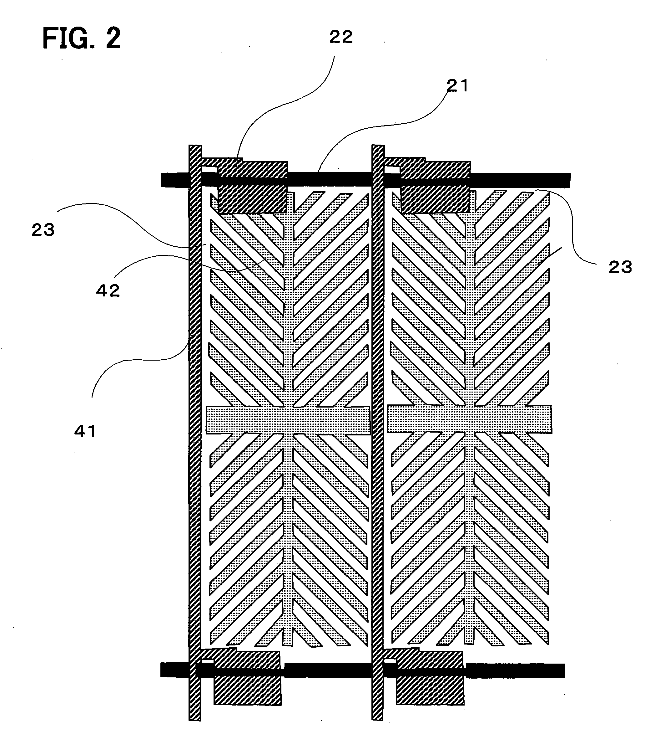
[0102] In comparative example 1 and embodimental examples 1 to 4, the liquid crystal panels were produced under the following conditions, unless otherwise stated. When using the electrode structure shown in FIG. 2 or FIG. 9, the width's of the electrodes and the slits in the pixel electrodes were respectively set to 3 μm.
[0103] A 15-type XGA liquid crystal panel was used, with vertical alignment control films coated on both substrates (not shown in the figure). A diacrylate monomer was used as a polymerizable compound. Active energy rays (i-line, 365 nm) were irradiated at room temperature while a voltage corresponding to the voltage for white display was applied.
[0104] The scanning electrodes, signal electrodes and pixel electrode were disposed ...
embodimental example 1
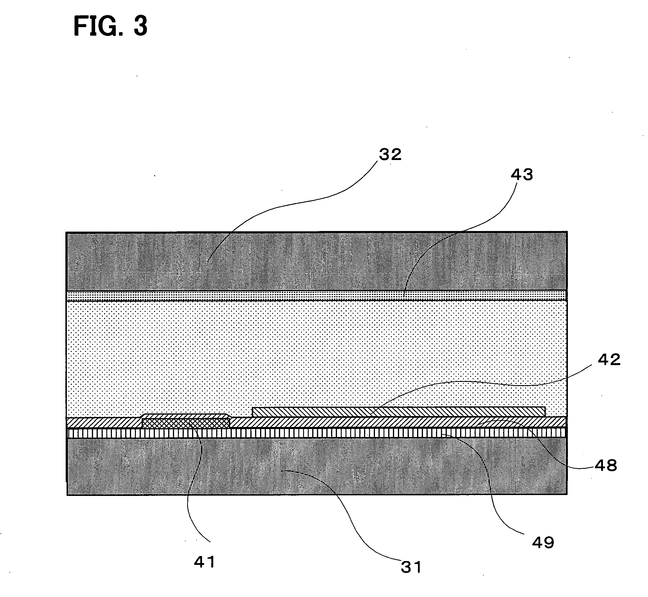
[0107] The structure shown in FIGS. 2 and 3 was adopted. When polymerizing the monomer, a voltage of 20 V was applied to the pixel electrodes, as well as 10 V, to the signal electrodes, and 0 V, to the counter electrode. To simplify the voltage application, the entire signal electrodes and the entire scanning electrodes were wired for them to be able to be gathered into a bundle or bundles at one or a few points so as to allow simultaneous voltage application, the bundle or bundles being cutoff after the polymerization of the monomer so that the bus lines were separated from each other.
[0108] As a result, irregularity in the alignment such as shown in the comparative example 1 was not produced. In this panel, a light-shielding film was disposed on parts of the counter electrode positioned opposite to the scanning electrodes and the vicinity thereof. Under this condition, a contrast value of 800 was obtained. The transmittance of the liquid crystal panel was improved by 15%, as comp...
embodimental example 2
[0109] The planar structure shown in FIG. 2 was combined with the cross-sectional structure shown in FIG. 11. The thickness of the added insulating layer 40 was 3 μm. An acryl resin was used as a material constituting the insulating layer 40.
[0110] When polymerizing the monomer, a voltage of 20 V was applied to the pixel electrodes and the signal electrodes, while 0 V was applied to the counter electrode. A layer was provided on the counter substrate for shielding the light in the vicinity of the scanning electrodes.
[0111] As a result, such irregularity in the alignment as shown in the comparative example 1 was not produced. Furthermore, a contrast value of 800 was obtained.
[0112] The transmittance of this liquid crystal panel was improved by 30%, as compared with the conventional MVA mode liquid crystal panels having large protrusions and large electrode slits.
[0113] It is to be noted that it may also be possible to make the added insulating layer have the role of a color filte...
PUM
| Property | Measurement | Unit |
|---|---|---|
| Percent by mass | aaaaa | aaaaa |
| Thickness | aaaaa | aaaaa |
| Weight | aaaaa | aaaaa |
Abstract
Description
Claims
Application Information