

Projection optical system and method
a projection optical system and optical system technology, applied in the field of projection optical systems, can solve the problems of increasing the weight and size of the projection optical system, and the range of challenges, and achieve the effects of improving the design of the immersion-type projection optical system, reducing size, and good imaging properties
- Summary
- Abstract
- Description
- Claims
- Application Information
AI Technical Summary
Benefits of technology
Problems solved by technology
Method used
Image

Examples
Embodiment Construction
[0074] In the exemplary embodiments described below, components that are alike in function and structure are designated as far as possible by alike reference numerals. Therefore, to understand the features of the individual components of a specific embodiment, the descriptions of other embodiments and of the summary of the invention should be referred to.
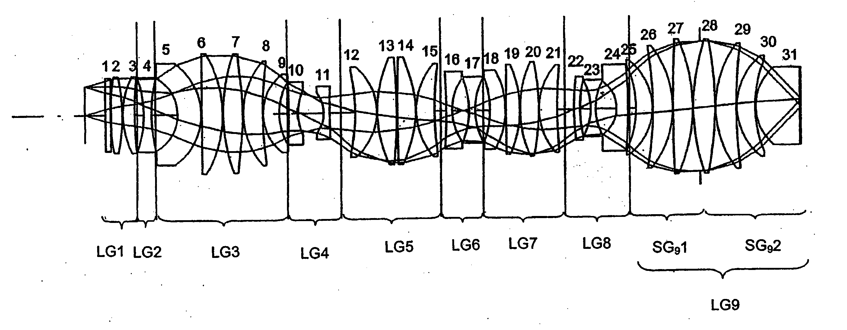
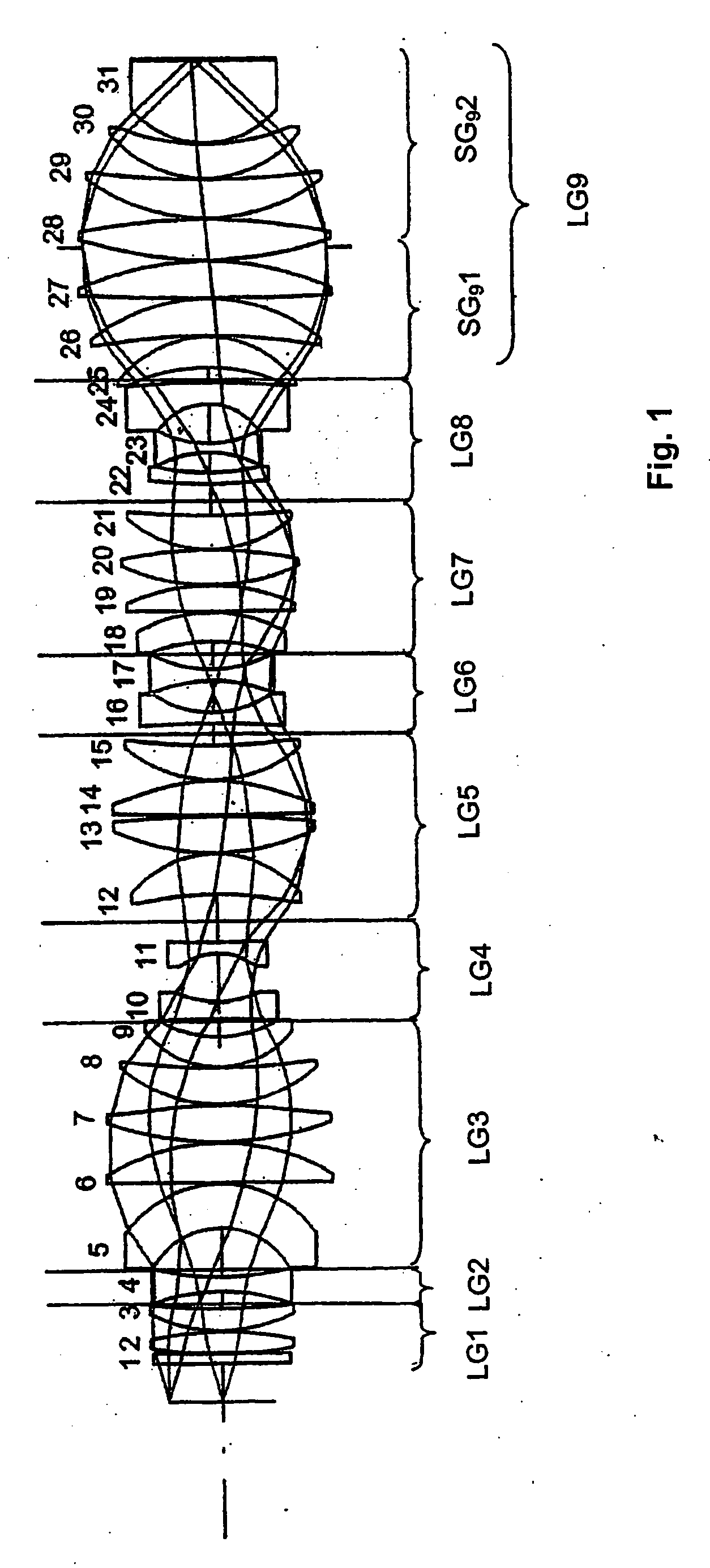
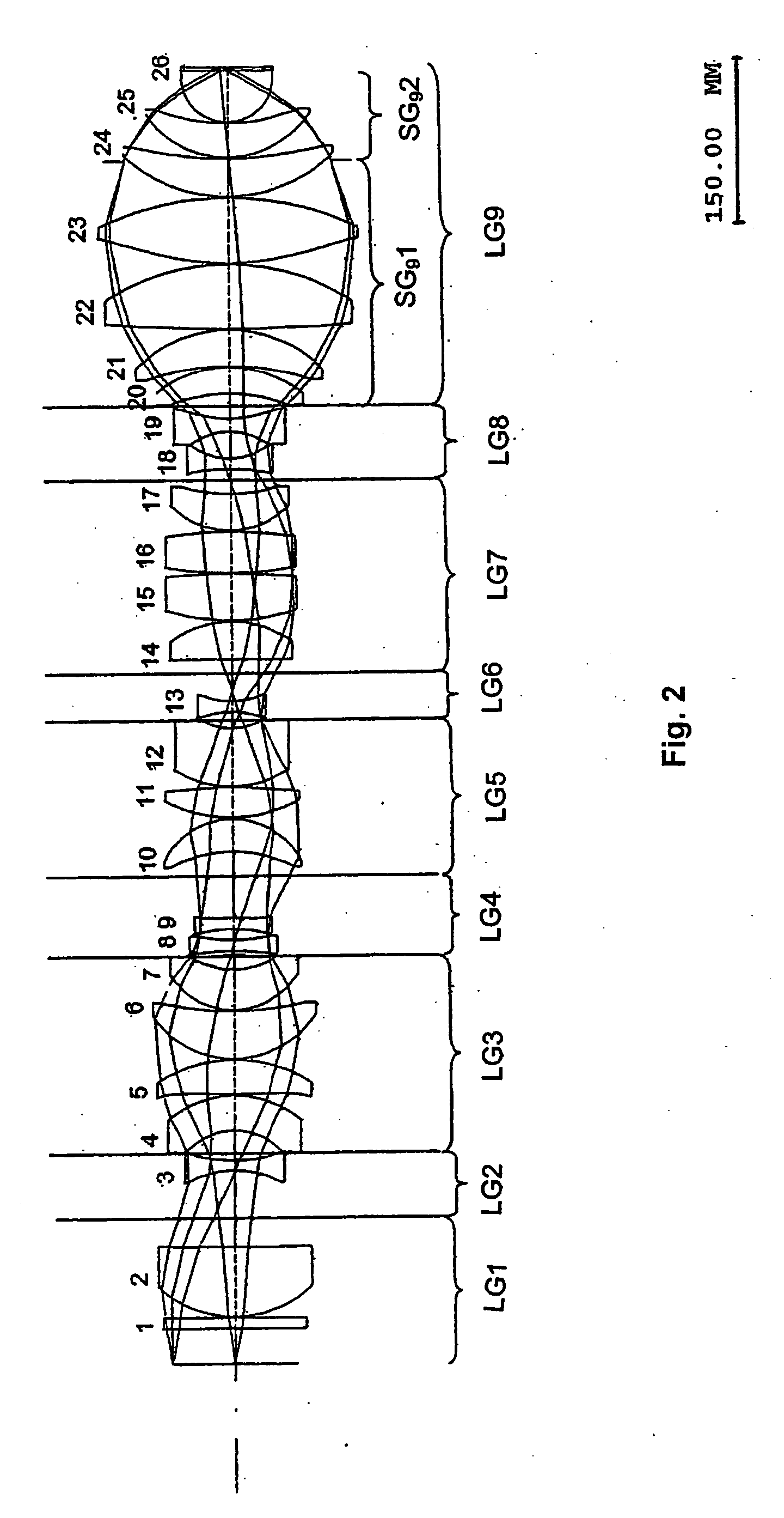
[0075] In FIG. 1, an optical path diagram of a first exemplary embodiment of a projection optical system according to the present invention is depicted. As indicated by the brackets, a first group of lenses LG1 includes four lenses 1, 2, 3 and has positive refractive power; a second group of lenses LG2 is formed of (single) lens 4 and has negative optical power; the third group of lenses LG3 includes five lenses 5, 6, 7, 8, 9 and has positive refractive power; the fourth group of lenses LG4 includes two lenses 10, 11 and has negative refractive power; the fifth group of lenses LG5 includes four lenses 12, 13, 14, 15 and has positiv...
PUM
 Abstract
Description
Claims
Application Information