Clock and data recovery circuit

a clock and data recovery technology, applied in pulse manipulation, pulse technique, synchronisation signal speed/phase control, etc., can solve the problems of large chip size, power consumption increase, and large chip size, and achieve improve jitter tolerance characteristics, and excellent jitter tolerance characteristics

Inactive Publication Date: 2006-03-16
RENESAS ELECTRONICS CORP
View PDF5 Cites 36 Cited by
  • Summary
  • Abstract
  • Description
  • Claims
  • Application Information

AI Technical Summary

Benefits of technology

[0016] In accordance with the present invention, a frequency tracking loop, a phase tracking loop and a feedback controller, with performs feedback control with respect to an integrator, are provided. As a result, it is possible to provide a clock and data recovery circuit that tracks frequency-modulated data and exhibits an excellent jitter tolerance characteristic. The reason for this is that it is possible to track frequency-modulated data by the action of the frequency tracking loop and to improve the jitter tolerance characteristic by the action of the feedback controller.
[0017] In accordance with the present invention, a clock and data recovery circuit exhibiting an excellent jitter tolerance characteristic can be provided by providing a phase tracking loop and a feedback controller that performs feedback control with respect to an integrator. The reason for this is that it is possible to improve the jitter tolerance characteristic by the action of the feedback controller.

Problems solved by technology

In a multichannel implementation, however, chip size and power consumption are great.
Specifically, when a clock and data recovery circuit having a frequency tracking loop that includes a charge pump, loop filter and VCO has a multichannel configuration, the frequency tracking loop including the charge pump, loop filter and VCO is provided in all of the channels, resulting in a large chip size.
Power consumption increases if a high-speed VCO is provided in all of the channels in a high-speed system of 1 Gbps or higher.
In such cases there may be a decline in the jitter tolerance characteristic in a certain frequency band.

Method used


Image

  • Clock and data recovery circuit
  • Clock and data recovery circuit
  • Clock and data recovery circuit

Examples


first embodiment

[0063] The structure and operation of the best mode for carrying out the present invention will now be described using-a specific embodiment.

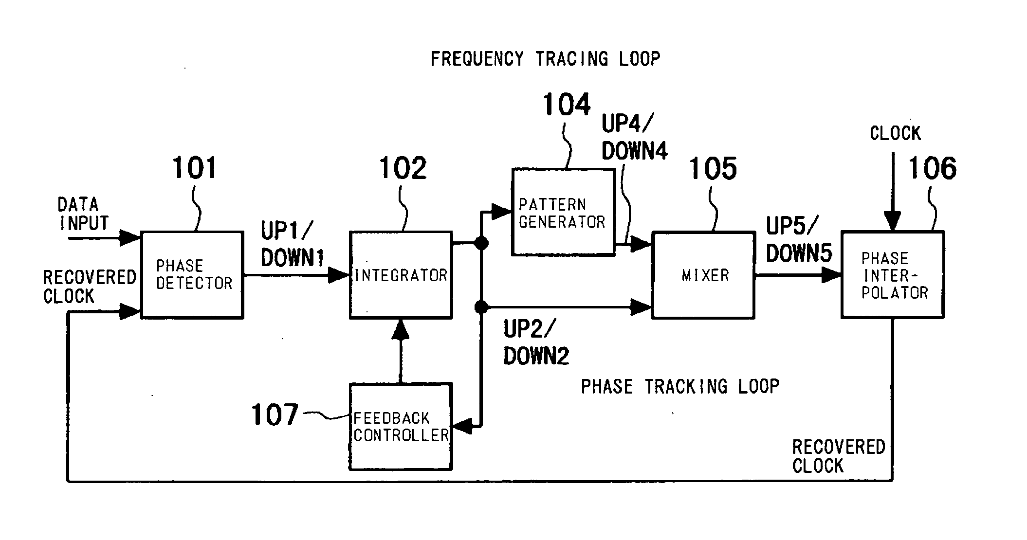
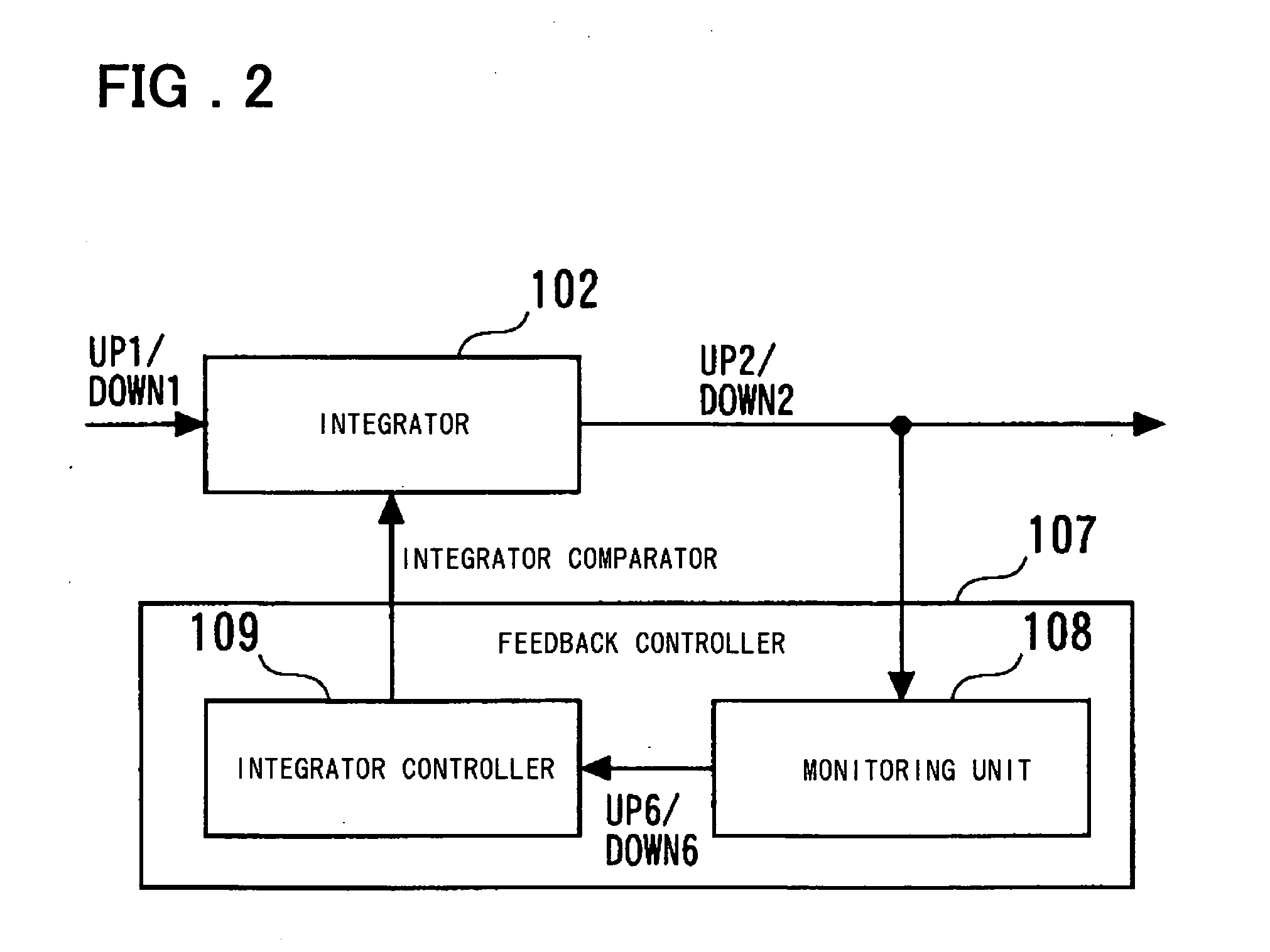
[0064]FIG. 7 is a diagram illustrating a transition in the state of the monitoring unit 108 in the feedback controller 107 shown in FIG. 2, and FIG. 8 is a diagram illustrating a transition in the state of the integrator controller 109.

[0065] In FIG. 2, the monitoring unit 108 is constituted by a counter, which is not shown. In FIG. 7, numerical values (−3 to +3) within the ovals representing state indicate the values (states) of the counter.

[0066] Assume that UP2=1 has been input to the monitoring unit 108. If the value in the counter at this time is equal to or greater than +0 and less than +2, then the value is incremented. If the value of the count is +3, the monitoring unit 108 returns the count to +0 and outputs DOWN6=1. If the value of the count is less than −0, the monitoring unit 108 updates this to +1 and outputs UP6=1.

[0067] Assu...


PUM


Abstract

A clock and data recovery circuit that tracks the frequency and phase fluctuation of serial data includes a feedback controller for monitoring tracking speed of an extraction clock with respect to the frequency and phase fluctuation of the serial data and applying feedback control to an integrator adaptively and moment to moment, thereby raising the tracking speed of the recovered clock and improving the jitter tolerance characteristic.

Description

FIELD OF THE INVENTION [0001] This invention relates to a clock and data recovery circuit and, more particularly, to a circuit for controlling tracking speed adaptively in a clock and data recovery circuit, which is mounted on an LSI device on the receiving side, when data is transferred serially between LSI devices. BACKGROUND OF THE INVENTION [0002] The development of semiconductor technologies in recent years has been accompanied by serialization of data transmission between LSI devices. There are instances where the operating clock frequency of a transmit LSI device and that of a receive LSI device coincide and instances where they do not. One example of a method adopted in a case where these frequencies do not coincide is to reduce EMI (EletroMagnetic Interference) using a spread spectrum clock in which frequency modulation is applied in the transmit LSI device. A method of extracting a clock signal from frequency-modulated serial data in the receive LSI device relies upon a kn...

Claims


Application Information

Patent Timeline
Patent Type & Authority Applications(United States)
IPC IPC(8): H03D3/24H03D3/18H04L27/06
CPCH03L7/0814H03L7/093H04L7/033H04L7/0025H04L7/0004
Inventor TAKEUCHI, MASAHIRO
Owner RENESAS ELECTRONICS CORP
Why Eureka
Try Eureka