Clock and data recovery circuit
a clock and data recovery technology, applied in pulse manipulation, pulse technique, synchronisation signal speed/phase control, etc., can solve the problems of large chip size, power consumption increase, and large chip size, and achieve improve jitter tolerance characteristics, and excellent jitter tolerance characteristics
- Summary
- Abstract
- Description
- Claims
- Application Information
AI Technical Summary
Benefits of technology
Problems solved by technology
Method used
Image
Examples
first embodiment
[0063]The structure and operation of the best mode for carrying out the present invention will now be described using-a specific embodiment.
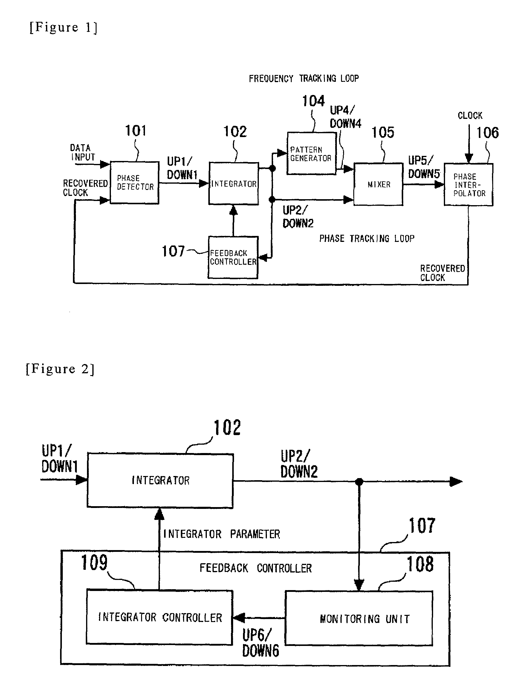
[0064]FIG. 7 is a diagram illustrating a transition in the state of the monitoring unit 108 in the feedback controller 107 shown in FIG. 2, and FIG. 8 is a diagram illustrating a transition in the state of the integrator controller 109.
[0065]In FIG. 2, the monitoring unit 108 is constituted by a counter, which is not shown. In FIG. 7, numerical values (−3 to +3) within the ovals representing state indicate the values (states) of the counter.
[0066]Assume that UP2=1 has been input to the monitoring unit 108. If the value in the counter at this time is equal to or greater than +0 and less than +2, then the value is incremented. If the value of the count is +3, the monitoring unit 108 returns the count to +0 and outputs DOWN6=1. If the value of the count is less than −0, the monitoring unit 108 updates this to +1 and outputs UP6=1.
[0067]Assume that ...
PUM
 Abstract
Description
Claims
Application Information


