Solder foil semiconductor device and electronic device

a semiconductor and foil technology, applied in the direction of semiconductor/solid-state device details, soldering apparatus, manufacturing tools, etc., can solve the problems of not being able to use temperature-hierarchical bonding, not being able to combine temperature-hierarchical bonding, and not being able to meet the requirements of high-temperature side temperature-hierarchical bonding, etc., to achieve the effect of new-type solder bonding

Inactive Publication Date: 2006-03-23
RENESAS ELECTRONICS CORP
View PDF9 Cites 72 Cited by
  • Summary
  • Abstract
  • Description
  • Claims
  • Application Information

AI Technical Summary

Benefits of technology

[0006] An object of the present invention is to provide a semiconductor device and an electronic device by quite a novel solder bonding, and particularly to provide solder bonding on the high temperature side in the temperature hierarchical bonding.

Problems solved by technology

Thus, solders for the hierarchical bonding, which can withstand such a soldering temperature, must have a melting point of at least 250° C., but actually any Pb-free solders for use on the high temperature side of temperature-hierarchical bonding, which can be used in combination thereof, is not yet available.
Sn-5Sb (melting point: 240°-232° C.) is a most possible Pb-free solder composition, but is not available for the temperature-hierarchical bonding because of melting thereof.
Au-20Sn (melting point: 280° C.) is known as a solder of higher temperature series, but it is so hard and expensive that its use is restricted to a narrow range.
Particularly in bonding Si chips to a material having a different coefficient of thermal expansion and also in bonding of large chips, the Au-20Sn solder is not available, because it is so hard as to break Si chips with high possibility.

Method used


Image

  • Solder foil semiconductor device and electronic device
  • Solder foil semiconductor device and electronic device
  • Solder foil semiconductor device and electronic device

Examples


Embodiment Construction

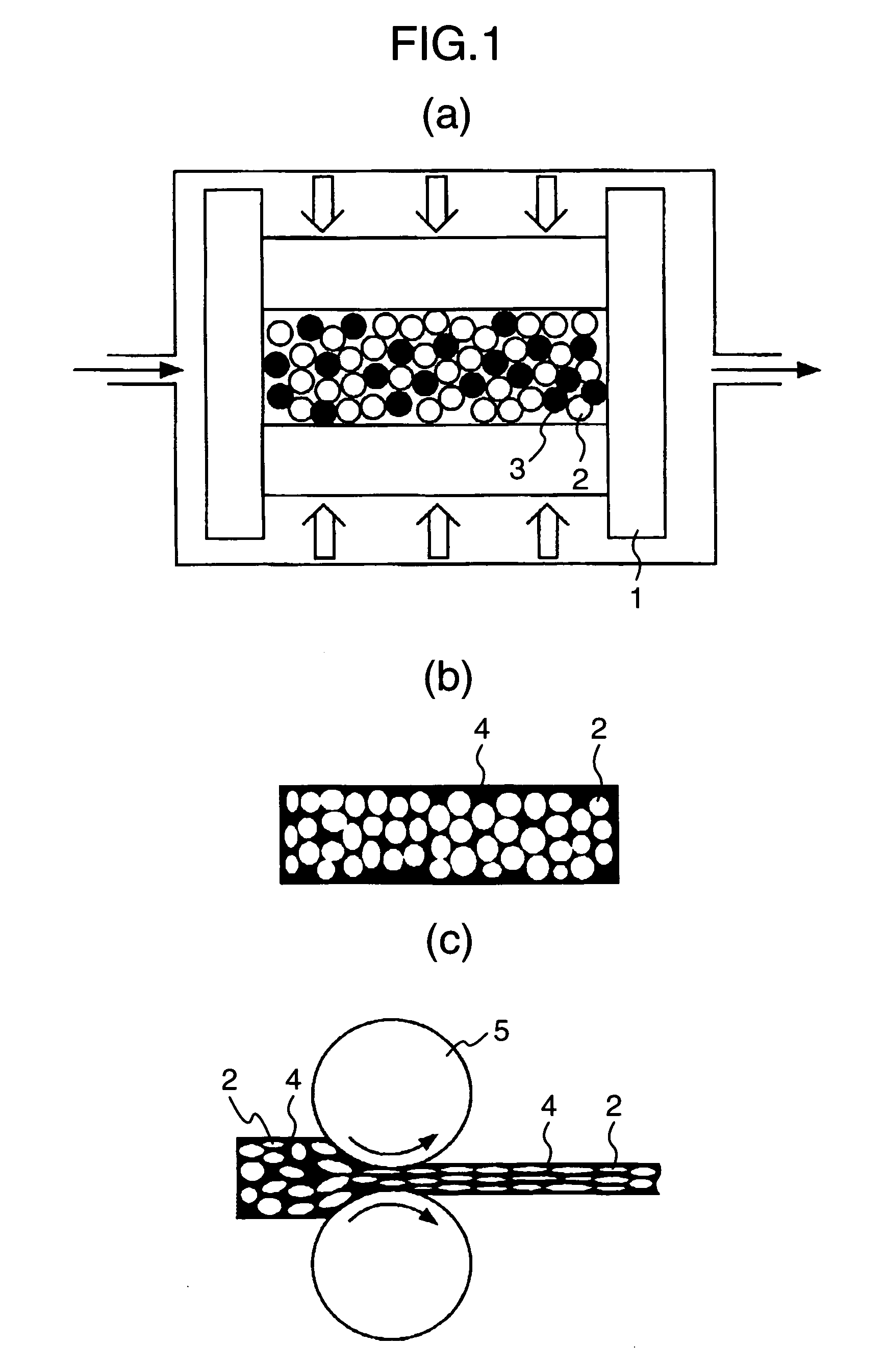
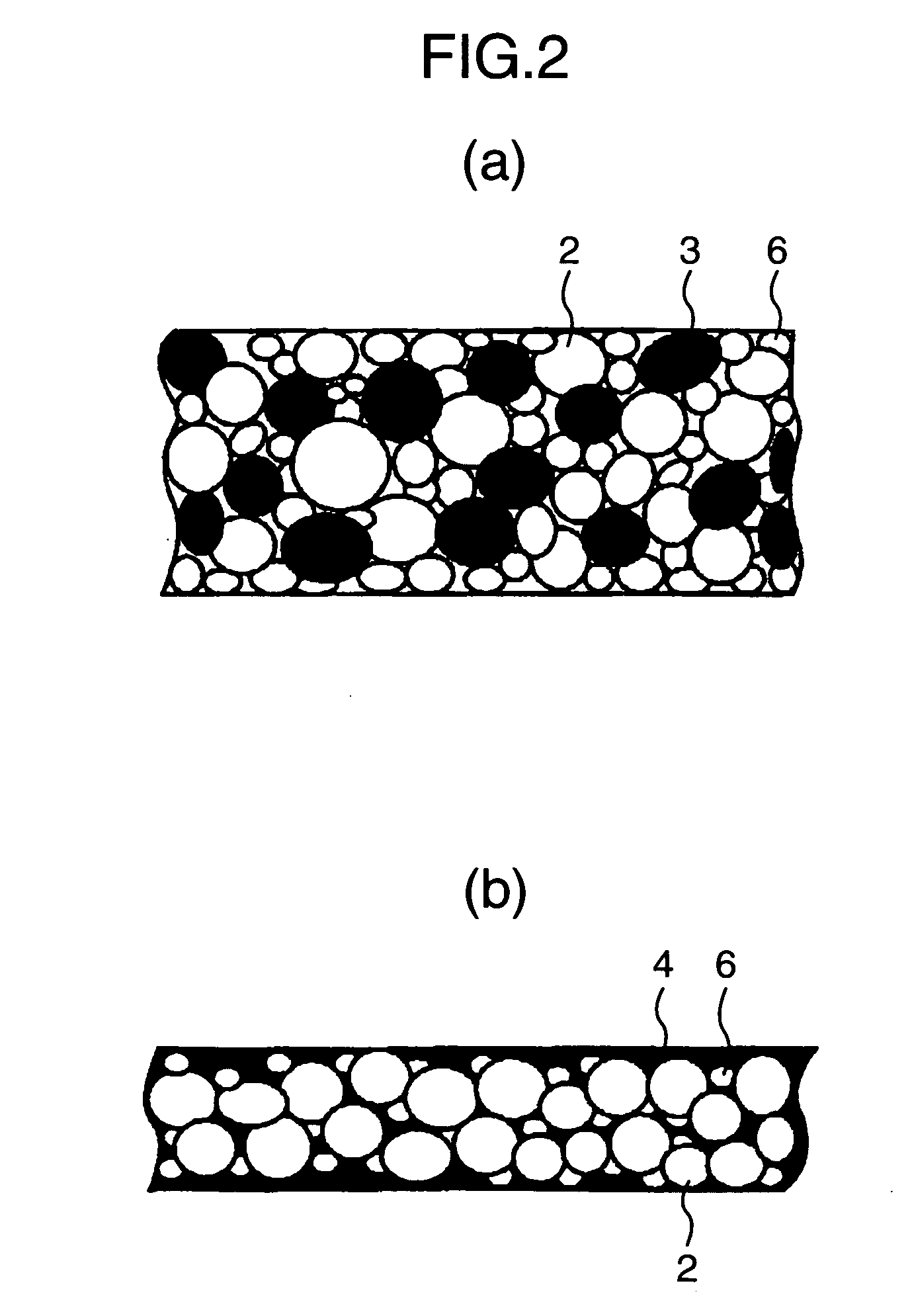
[0030] Among the inventions disclosed herein to attain the aforementioned objects, typical ones are briefly outlined below: [0031] (1) A solder foil formed from a material comprising metal particles and solder particles by rolling. [0032] (2) A solder foil formed from a solder material comprising Cu particles and Sn particles by rolling. [0033] (3) A solder foil formed from a solder comprising Cu and Sn by pressing, where Cu is in a particulate state and Sn is in a state of filling interspaces between the Cu particles. [0034] (4) A solder foil as described in said item (2) or (3), wherein when the solder foil is subjected to reflowing at least one portion of the Cu particle surfaces is covered by Cu6Sn5. [0035] (5) A solder foil as described in said item (2) or (3), wherein when the solder foil is subjected to reflowing the Cu particles and the Sn after plastic deformation are bonded to each other by a compound comprising Cu6Sn5. [0036] (6) A solder foil as described in said items (...


PUM

PropertyMeasurementUnit
particle sizesaaaaaaaaaa
melting pointaaaaaaaaaa

Abstract

A solder foil formed from a material comprising particles of Cu, etc. as metal particles and Sn particles as solder particles by rolling is suitable for solder bonding at a high temperature side in temperature-hierarchical bonding, and semiconductor devices and electronic devices produced by use of such solder bonding have distinguished reliability of mechanical characteristics, etc.

Description

TECHNICAL FIELD [0001] The present invention relates to a solder foil formed from a material comprising metal particles such as copper (Cu) particles or balls and solder particles such as tin (Sn) particles or balls by rolling, and a semiconductor device and an electronic device using the solder foil. BACKGROUND ART [0002] In the case of solders of Sn—Pb system, it has been possible to carry out temperature-hierarchical bonding, which comprises soldering lead (Pb)-rich Pb-5Sn (melting point: 314-310° C.), Pb-10Sn (melting point: 302-275° C.), etc. as high temperature series solders at temperatures of approximately 330° C., and then bonding a Sn-37Pb eutectic mixture (melting point: 183° C.) as low temperature series solders without melting the first soldered portions. These solders have been capable of bonding Si chips, etc., which are flexible and high in deformability and thus is easy to break, to a substrate having a different coefficient of thermal expansion. Such a temperature-...

Claims


Application Information

Patent Timeline
Patent Type & Authority Applications(United States)
IPC IPC(8): H05K1/16H01L23/48H05K1/14B23K3/06B23K35/14H05K3/34
CPCH01L2924/0132H01L24/75H01L2224/29H01L2224/2919H01L2924/01006H01L2924/01019H01L2924/01024H01L2924/014H01L2924/0665H01L2224/29101H01L2924/0133H01L2924/0134H01L2224/29109H01L2224/29111H01L2224/45124H01L2924/15724H01L2924/15747H01L2924/1579H01L2924/00013H01L2924/00011H01L2224/29499H01L2224/0401H01L2224/29076Y10T428/12528Y10T428/12708Y10T428/12903B23K3/063B23K2201/40H01L24/01H01L24/27H01L24/29H01L24/33H01L24/83H01L2224/04026H01L2224/16225H01L2224/32225H01L2224/32245H01L2224/45144H01L2224/48091H01L2224/48227H01L2224/48247H01L2224/49171H01L2224/73265H01L2224/8319H01L2224/83801H01L2924/01003H01L2924/01004H01L2924/01005H01L2924/01012H01L2924/01013H01L2924/01014H01L2924/01027H01L2924/01029H01L2924/0103H01L2924/01032H01L2924/01033H01L2924/01039H01L2924/01042H01L2924/01046H01L2924/01047H01L2924/0105H01L2924/01051H01L2924/01074H01L2924/01075H01L2924/01078H01L2924/01079H01L2924/01082H01L2924/01322H01L2924/01327H01L2924/09701H01L2924/10253H01L2924/10329H01L2924/13091H01L2924/15311H01L2924/15787H01L2924/16152H01L2924/166H01L2924/19041H01L2924/19043H01L2924/19105H05K3/3478H05K2201/0215H05K2203/0143H05K2203/0278H05K2203/0405H05K2203/0425H01L2924/01028H01L2224/83101H01L2224/29311H01L2224/29347H01L2924/00014H01L2924/05432H01L2924/00H01L2924/01007H01L2924/01031H01L2924/01022H01L2924/01026H01L2924/01049H01L2924/01083H01L2924/00012H01L2924/3512H01L2224/13111H01L2224/29099H01L2224/29199H01L2224/29299H01L2224/2929H01L2224/29298H01L2224/29211H01L2924/181H01L24/73H01L2224/292B23K2101/40H01L21/60
Inventor SOGA, TASAOHATA, HANAEISHIDA, TOSHIHARUISHIDA, KANKONAKATSUKA, TETSUYAOKAMOTO, MASAHIDEMIURA, KAZUMA
Owner RENESAS ELECTRONICS CORP
Why Eureka
Try Eureka