Semiconductor package with wire bond arrangement to reduce cross talk for high speed circuits

a high-speed circuit and wire bonding technology, applied in the direction of semiconductor devices, semiconductor/solid-state device details, electrical apparatus, etc., can solve the problems of device failure, reduce the total number of usable signal input-output pins on the package, etc., to reduce signal cross talk, and reduce signal cross talk between the wires

Inactive Publication Date: 2006-03-30
LSI CORPORATION
View PDF5 Cites 7 Cited by
  • Summary
  • Abstract
  • Description
  • Claims
  • Application Information

AI Technical Summary

Benefits of technology

[0007] The present invention relates to a semiconductor package for reducing signal cross talk between wire bonds of a semiconductor packages. The package includes a semiconductor die having a plurality of bond pads formed thereon. The bond pads are arranged in a first subset of bond pads and a second subset of bond pads. The package also includes a substrate having a plurality of contact points, the plurality of contact points are arranged in a first subset of contact points and a second subset of contact points. To reduce signal cross talk, the wire bonds are arranged such that a first subset of wire bonds are electrically coupled between the first subset of bond pads and the first subset of the contact points. The first subset of wire bonds have ball bonds formed on the first subset of bond pads and stitch bonds formed on the first subset of contact points respectively. A second subset of wire bonds are electrically coupled between the second subset of bond pads and the second subset of the contact points. The second subset of wire bonds have stitch bonds formed on the first subset of bond pads and ball bonds formed on the first subset of contact points respectively. The different height profiles of the first set and the second set of wire bonds tends to reduce signal cross talk between the wires.

Problems solved by technology

The closeness of the wires may create a problem.
Namely, coupling noise and cross talk between the wires may cause false signal transitions on the signal input-output pins, causing the device to fail.
The faster switching speeds of the transistors further exasperates this problem.
The problem with this approach is that it reduces the total number of usable signal input-output pins on the package.

Method used


Image

  • Semiconductor package with wire bond arrangement to reduce cross talk for high speed circuits
  • Semiconductor package with wire bond arrangement to reduce cross talk for high speed circuits

Examples


Embodiment Construction

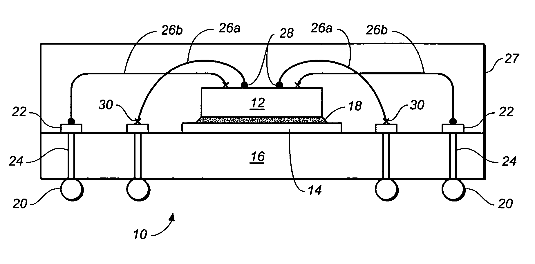
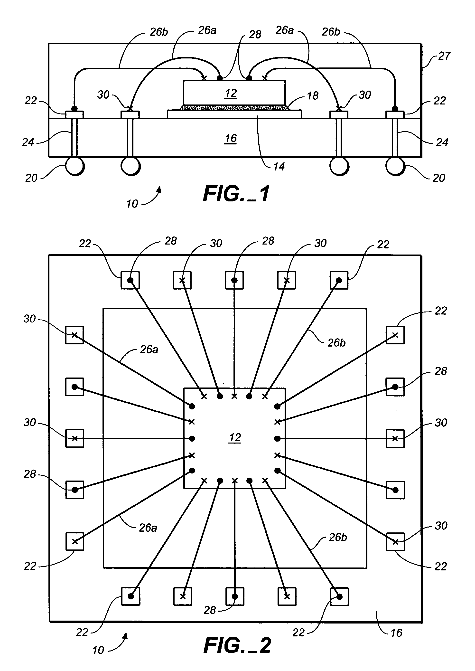
[0012] Referring to FIG. 1, a cross section of a package of the present invention is shown. The package 10 includes a semiconductor die 12 mounted onto a die attach area 14 of a substrate 16. A die attach material 18, such as an epoxy, is used to attach the die 12 to the die attach area 14. A plurality of solder ball contacts 20 are formed on the bottom surface of the substrate 16. The solder ball contacts 20 are electrically coupled to a plurality of contact points 22 on the top surface of the substrate 16 through vias 24. Although not visible in FIG. 1, the die 12 has a plurality of bond pads formed on the upper or active surface. Wire bonds 26 are formed between the bond pads on the die 12 and the contact points 22 on the substrate 16. The package is encapsulated in an encapsulant material 27.

[0013] In accordance with the present invention, the wire bonds 26 are arranged in a first subset 26a and a second subset 26b. [0014] 1. The bond wires 26a of the first subset are electrica...


PUM


Abstract

A package for reducing signal cross talk between wire bonds of semiconductor packages. The package includes a semiconductor die having a plurality of bond pads formed thereon. The bond pads arranged in a first subset of bond pads and a second subset of bond pads. The package also includes a substrate having a plurality of contact points, the plurality of contact points are arranged in a first subset of contact points and a second subset of contact points. To reduce signal cross talk, the wire bonds are arranged such that a first subset of wire bonds are electrically coupled between the first subset of bond pads and the first subset of the contact points. The first subset of wire bonds have ball bonds formed on the first subset of bond pads and stitch bonds formed on the first subset of contact points respectively. A second subset of wire bonds are electrically coupled between the second subset of bond pads and the second subset of the contact points. The second subset of wire bonds have stitch bonds formed on the first subset of bond pads and ball bonds formed on the first subset of contact points respectively. The different height profiles of the first set and the second set of wire bonds tends to reduce signal cross talk between the wires.

Description

BACKGROUND OF THE INVENTION [0001] 1. Field of the Invention [0002] The present invention relates generally to semiconductor packaging, and more particularly, to a semiconductor package with a wire bond arrangement to reduce cross talk between the wires. [0003] 2. Description of the Related Art [0004] Advances in processing technology has allowed engineers to fabricate smaller and smaller transistors. The smaller transistors not only operate at faster speeds, but they also enable more and more transistors to be fabricated on a semiconductor die of a given size. This increased circuit density has enabled circuit designers to add greater functionality with each new generation of chips. The new functionality, however, increases the need for a greater number of signal inputs as well as power and ground inputs to the device. State of the art chip packages currently have hundreds and in some instances thousands of input-output pins. The increased number of input-output pins results in the...

Claims


Application Information

Patent Timeline
Patent Type & Authority Applications(United States)
IPC IPC(8): H01L23/52
CPCH01L23/49838H01L2224/32225H01L24/85H01L2223/6611H01L2224/48091H01L2224/48095H01L2224/48227H01L2224/48465H01L2224/48471H01L2224/49052H01L2224/49171H01L2224/4943H01L2224/4945H01L2224/73265H01L2224/85191H01L2924/01029H01L2924/01082H01L2924/15311H01L2924/3025H01L24/49H01L2924/014H01L2924/01033H01L2924/00014H01L2224/78H01L2924/00H01L2924/00012H01L24/48H01L24/73H01L2924/181H01L2224/45099H01L2224/05599
Inventor CHIA, CHOK J.LIEW, WEE KEONGLIM, SENG SOOI
Owner LSI CORPORATION
Why Eureka
Try Eureka