Method for forming isolation grooves among pixels of CMOS (complementary metal oxide semiconductor) image sensor

A technology for image sensors and isolation trenches, applied in semiconductor/solid-state device manufacturing, electrical components, circuits, etc., can solve the problems of large leakage current of semiconductor devices, affecting the photoelectric characteristics of CMOS image sensors, and destroying substrates

Inactive Publication Date: 2015-02-11
WUHAN XINXIN SEMICON MFG CO LTD
View PDF8 Cites 3 Cited by
  • Summary
  • Abstract
  • Description
  • Claims
  • Application Information

AI Technical Summary

Problems solved by technology

[0008] In view of the above problems, the present invention provides a method for forming isolation trenches between pixels of a CMOS image sensor to solve the problem in the prior art that during the dry etching process, hig

Method used


Image

  • Method for forming isolation grooves among pixels of CMOS (complementary metal oxide semiconductor) image sensor
  • Method for forming isolation grooves among pixels of CMOS (complementary metal oxide semiconductor) image sensor
  • Method for forming isolation grooves among pixels of CMOS (complementary metal oxide semiconductor) image sensor

Examples


Embodiment Construction
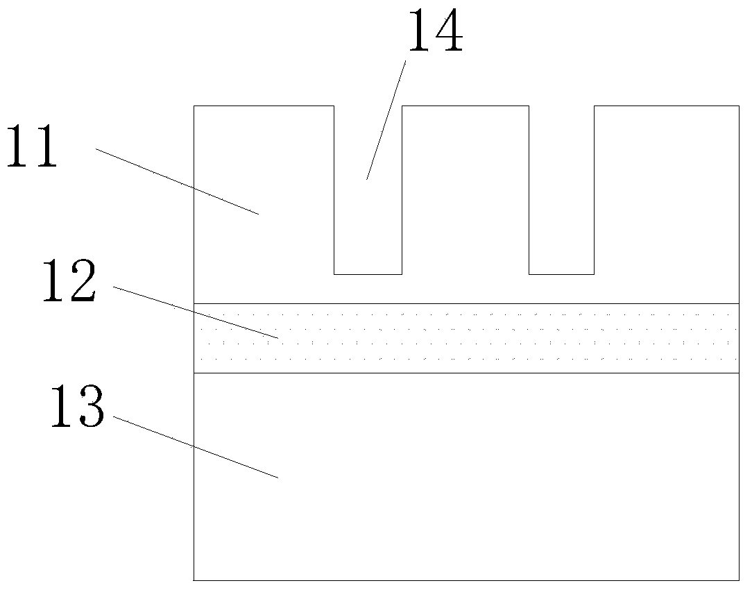
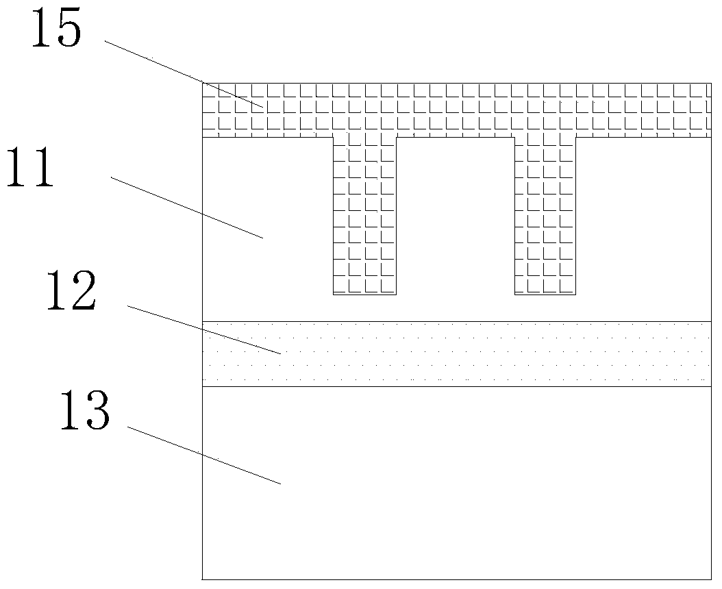
[0033] The core idea of ​​the present invention is: cover a barrier layer on the upper surface of a bonded wafer, and use lithography process and first wet etching process to etch a number of pattern windows on the barrier layer, and use the barrier layer A second wet etching process is performed on the wafer for the mask to replace the traditional dry etching process, several isolation trenches are formed in the wafer and subsequent oxide filling is performed.

[0034] The present invention will be further described below in conjunction with the accompanying drawings and specific embodiments, but not as a limitation of the present invention.

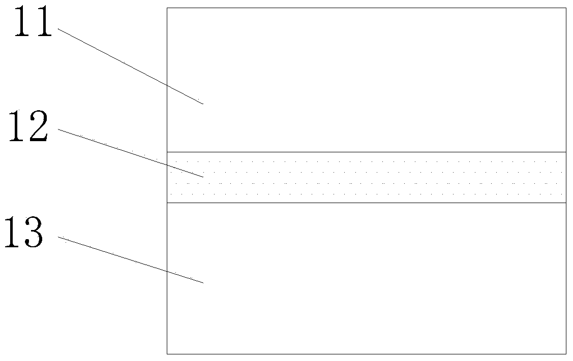
[0035] Step S1, preparing a bonded wafer, the bonded wafer includes a first wafer and a second wafer, the first wafer is located above the second wafer, and the front surfaces of the two wafers are bonded to each other, specifically , the first wafer includes a first substrate 21 and a first BEOL dielectric layer 22, and the second wafe...


PUM


Abstract

The invention relates to the technical field of semiconductor manufacturing, in particular to a method for forming isolation grooves among pixels of a CMOS (complementary metal oxide semiconductor) image sensor. According to the method, a blocking layer covers the surface of a bonded wafer, in addition, a lithography process and a first wet process etching process are adopted for etching a plurality of pattern windows in the blocking layer, in addition, the blocking layer is used as a mask for carrying out second wet process etching process processing on the wafer for replacing the traditional dry process etching process, a plurality of isolation grooves are formed, and subsequent oxide injection is carried out. According to the technical scheme, the problem of great electricity leakage current of a semiconductor device due to substrate damage caused by high-energy ion bombardment in the process of the traditional dry process etching process can be avoided, so the signal cross talk among the pixels of the CMOS image sensor can be reduced, and the photoelectric characteristics of the CMOS image sensor are enhanced.

Description

technical field [0001] The invention relates to the technical field of semiconductor manufacturing, in particular to a method for forming isolation trenches between pixels of a CMOS image sensor. Background technique [0002] With the continuous maturity and development of semiconductor manufacturing technology, CMOS image sensors are increasingly used in digital cameras, PC Cameras, video phones, third-generation mobile phones, video conferencing, intelligent security systems, car reversing sensors, toys and industrial, medical and other fields. [0003] CMOS image sensor belongs to optoelectronic components, because its manufacturing process is compatible with the existing integrated circuit manufacturing process, and its performance has many advantages over the original charge-coupled device (CCD), and it has gradually become the mainstream of image sensors. The driving circuit and the pixel can be integrated together, which simplifies the hardware design and reduces the...

Claims


Application Information

Patent Timeline
IPC IPC(8): H01L27/146H01L21/762
Inventor 董金文朱继锋肖胜安胡思平
Owner WUHAN XINXIN SEMICON MFG CO LTD
Why Eureka
Try Eureka