

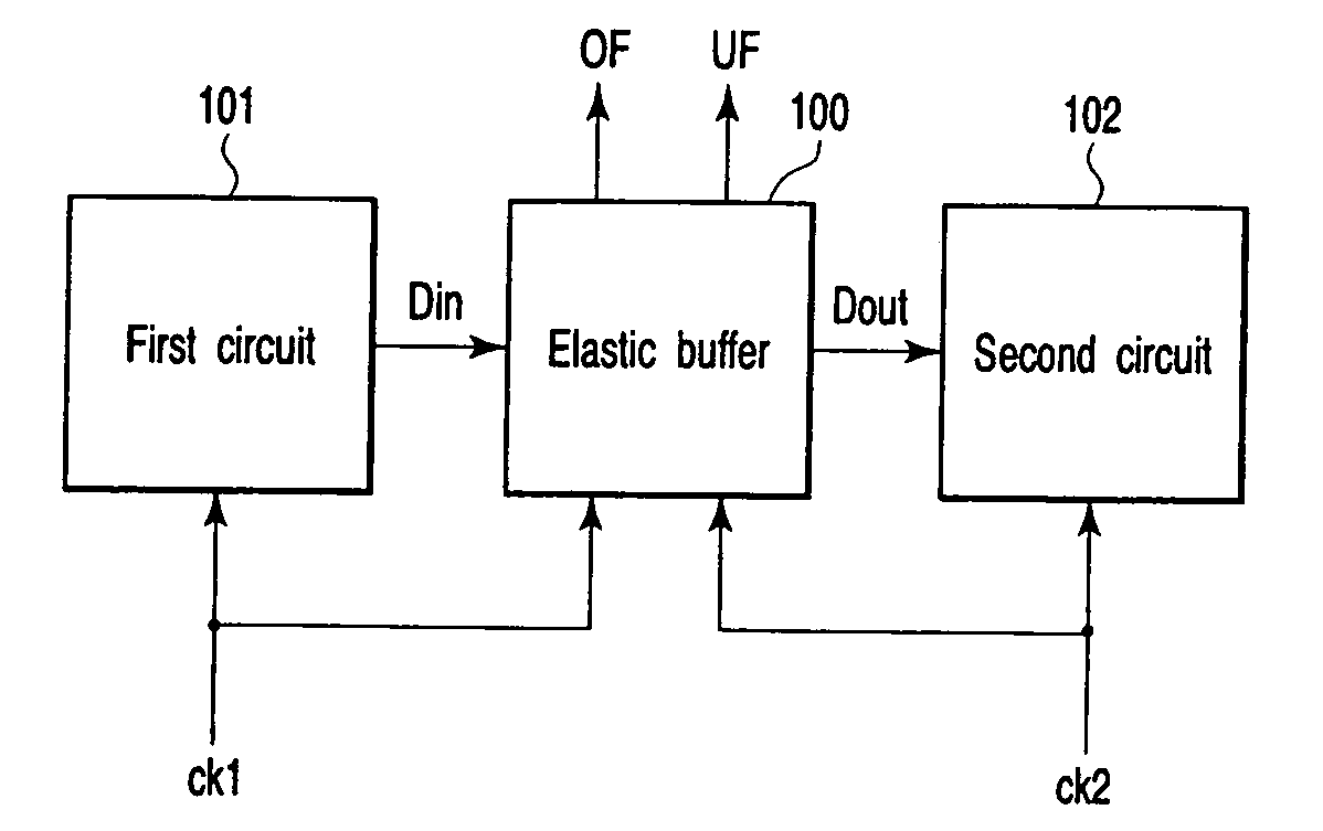
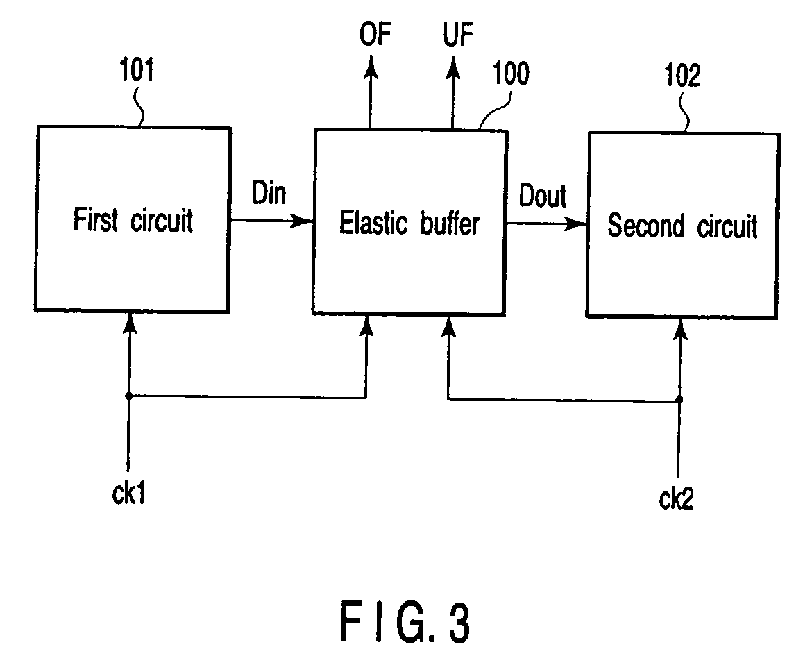
Elastic buffer
a buffer and elastic technology, applied in the field of elastic buffers, can solve problems such as accidental overtaking, destruction of unread data,
- Summary
- Abstract
- Description
- Claims
- Application Information
AI Technical Summary
Problems solved by technology
Method used
Image

Examples
first embodiment
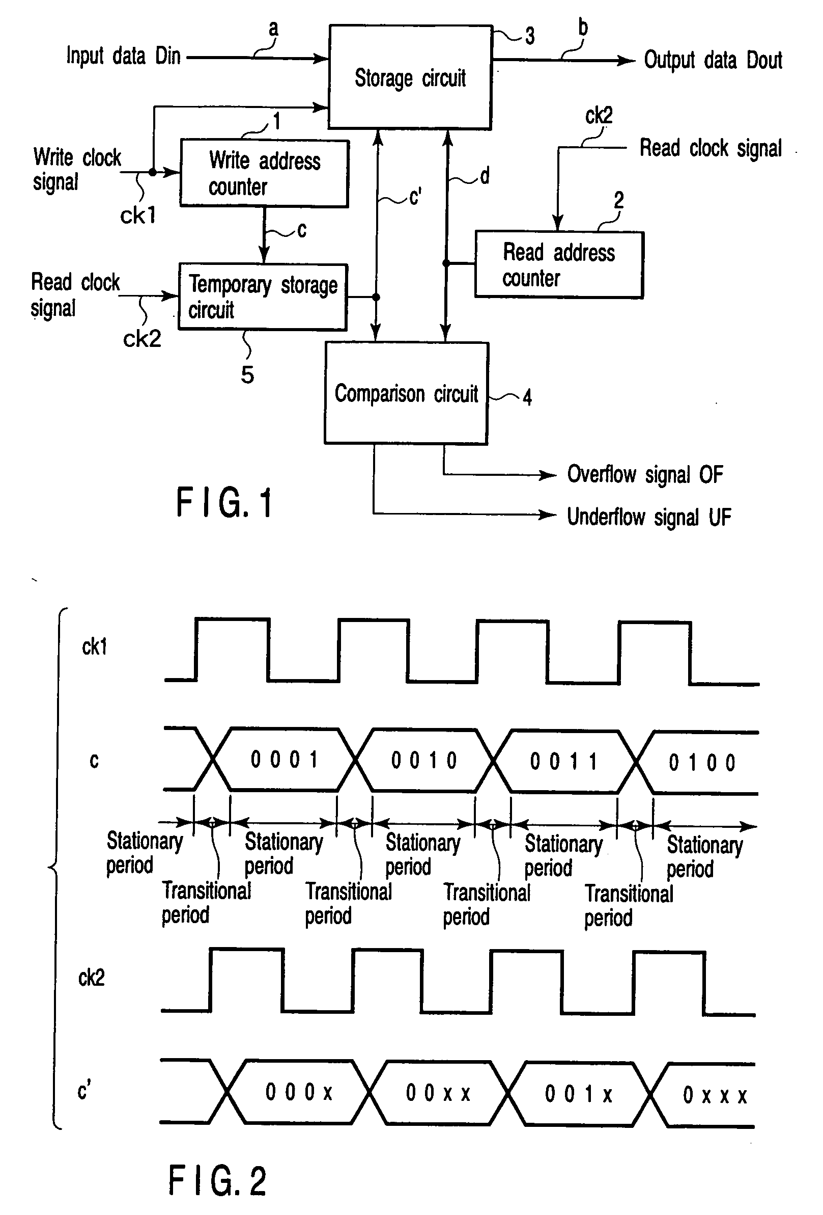
[0050]FIG. 4 shows an elastic buffer according to a first embodiment of the invention. The elastic buffer has the write address counter 1, the read address counter 2, the first-in first-out (FIFO) storage circuit 3, ring counters 6a to 6c, a temporary storage circuit 7, AND circuit groups 8a and 8b which are respectively formed from a plurality of AND circuits, OR circuits 9a and 9b, storage circuits 10a and 10b, and a decode circuit 11.
[0051] Input data Din and the write clock ck1 are input to the data port and the clock input port of the storage circuit 3. Output data Dout is output from the data output port of the storage circuit 3. The write address counter 1 generates a write address c so as to synchronize the write clock signal ck1. The read address counter 2 generates a read address d so as to synchronize the read clock signal ck2. The write address c and the read address d are input to the storage circuit 3.
[0052] The storage circuit 3 writes the input data Din into a writ...
second embodiment
[0098]FIG. 16 shows another concrete configuration of the decode circuit 11 in FIG. 4. The decode circuit 11 shown in FIG. 4 is constituted of two AND circuits 17a and 17b with three inputs. The signals m, n, o, p, UF, and OF in FIG. 16 correspond to those in FIG. 4. The output signal m of the OR circuit 9a, the output signal n of the OR circuit 9b, and the output signal o of the storage circuit 10a are input to the AND circuit 17a. The output signal m of the OR circuit 9a, the output signal n of the OR circuit 9b, and the output signal p of the storage circuit 10b are input to the AND circuit 17b.
[0099] Table 3 is a truth table corresponding to the decode circuit shown in FIG. 16. Slipping-through the trap by the pattern to be detected ‘x1x’ in the data stored in the temporary storage circuit 7 is permitted in the truth table serving as the above Table 2, and on the other hand, slipping-through the ideal position is permitted in the Table 3. However, the ideal position is required...
third embodiment
[0103]FIG. 17 shows an elastic buffer according to a third embodiment of the invention. Note that, in FIG. 17, portions corresponding to those in FIG. 4 described above are denoted by the same reference numerals, and descriptions thereof will be omitted. Hereinafter, only portions different from those in FIG. 4 will be described. In the elastic buffer of FIG. 17, a decode circuit 18 different from the decode circuit 11 in FIG. 4 is provided, and two storage circuits 19a and 19b are newly added.
[0104] The decode circuit 18 outputs an underflow signal UF and an overflow signal OF. The underflow signal UF and the overflow signal OF are respectively input to the storage circuits 19a and 19b. Output signals from the storage circuits 19a and 19b are respectively input as state signals u and v to the decode circuit 18. The decode circuit 18 decodes the signals u and v along with the signals m, n, o, and p.
[0105] As the decode circuit 18 in FIG. 17, for example, a circuit shown in FIG. 18...
PUM
 Abstract
Description
Claims
Application Information