Eureka AIR delivers breakthrough ideas for toughest innovation challenges, trusted by R&D personnel around the world.

Plasma display device and method for driving the same

Inactive Publication Date: 2006-04-13
SAMSUNG SDI CO LTD
View PDF4 Cites 4 Cited by
  • Summary
  • Abstract
  • Description
  • Claims
  • Application Information

AI Technical Summary

Benefits of technology

[0007] The present invention provides a method for driving a plasma display device, which reduces the luminance of sub-fields having smaller weights to improve representation of lower gray scale.

Problems solved by technology

When a lower gray scale, that is, a dark part, is represented in a display device, the lower gray scale is distinctly deteriorated when the luminance of the lower gray scale is excessively high.
Accordingly, even when the number of sustain discharge pulses is reduced, there is a limitation in decreasing the light intensity.
Particularly, emission efficiency has been improved recently to result in excessively high light intensity caused by one-time sustain discharge or address discharge.

Method used


Image

  • Plasma display device and method for driving the same
  • Plasma display device and method for driving the same
  • Plasma display device and method for driving the same

Examples


first embodiment

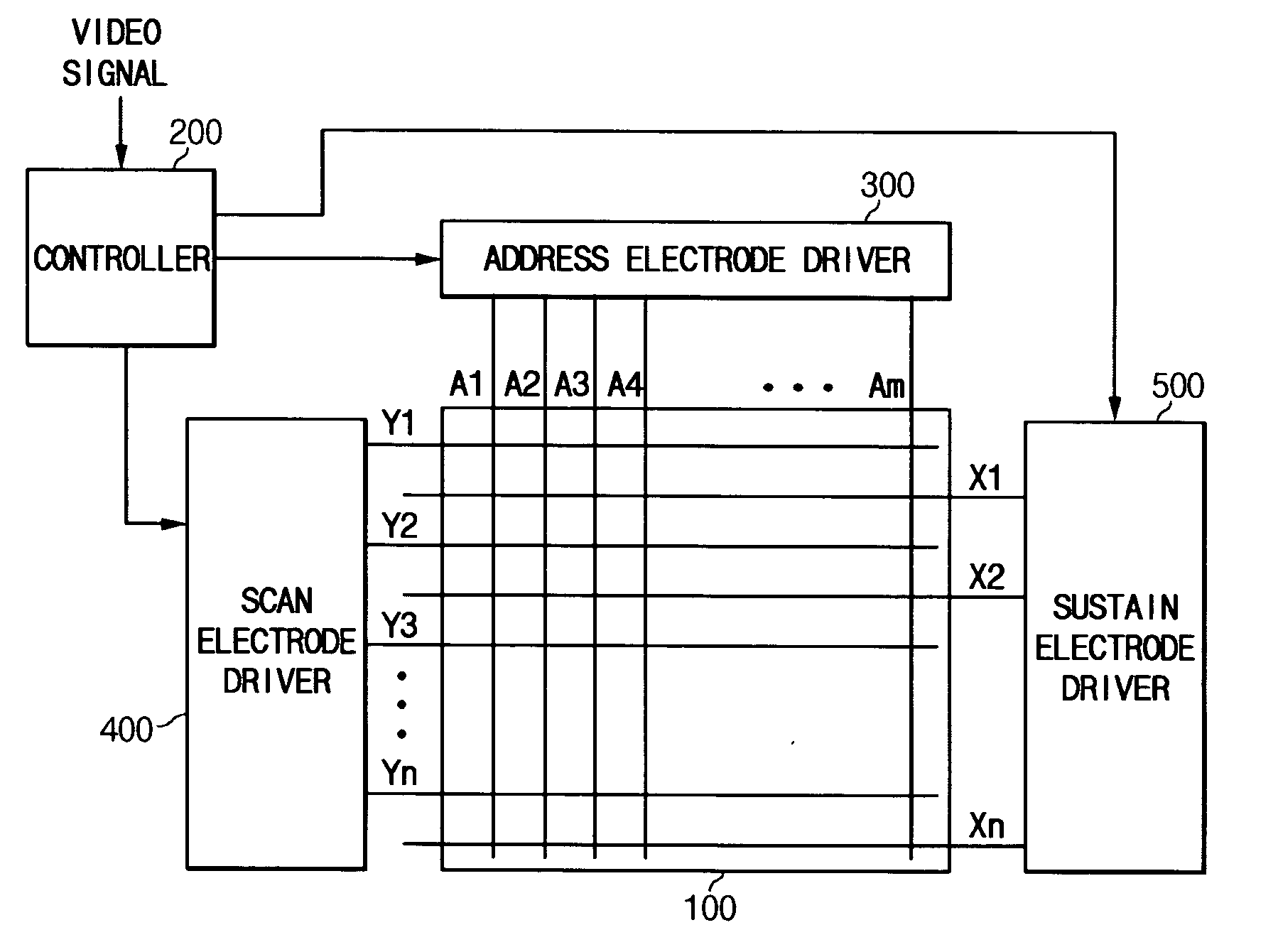
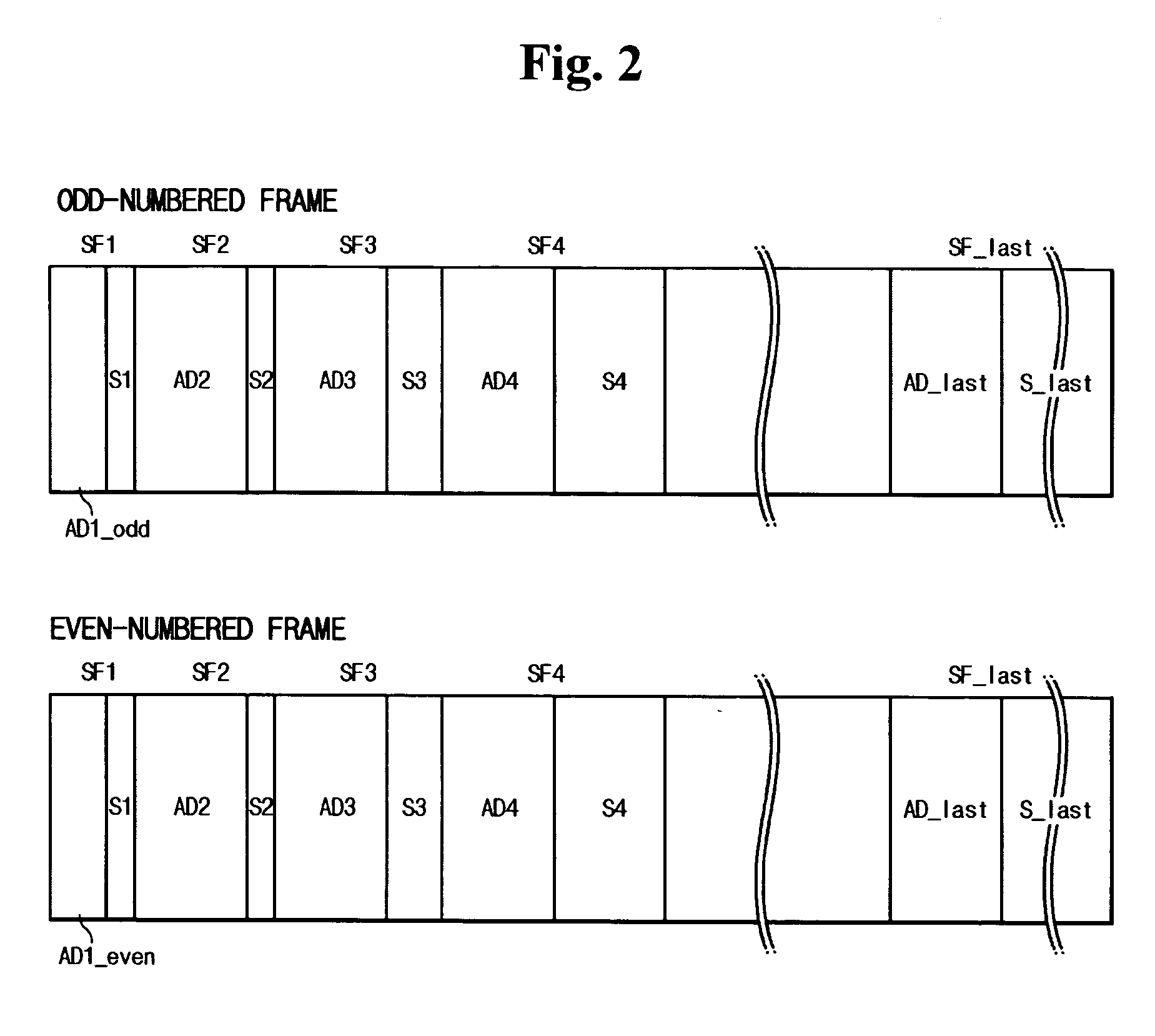
[0027] In the present invention, the controller 200 transmits control signals to the A electrode driver 300 and the Y electrode driver 500 such that the addressing operation is executed only for odd-numbered row electrodes or even-numbered row electrodes among the plurality of row electrodes in the address period AD1_odd or AD_even of the sub-field SF1 having the minimum weight. In addition, the controller 200 selects lit cells in the even-numbered row electrodes in even-numbered frames if lit cells are selected in the odd-numbered row electrodes in an odd-numbered frame, for example. That is, the Y electrode driver 500 selectively applies the scan pulse only to odd-numbered Y electrodes Y1, Y3, . . . , Yn−1 in the address period AD1_odd of the sub-field SF1 with the minimum weight of an odd-numbered frame, and selectively applies the scan pulse only to even-numbered Y electrodes Y2, Y4, . . . , Yn in the address period AD1_even of the sub-field SF1 with the minimum weight of an eve...

second embodiment

[0033] Referring to FIG. 3, in the address period AD1 of the sub-field SF1 of an odd-numbered frame, the Y electrode driver 500 selectively applies the scan pulse to the Y electrodes Y1 to Yn while the A electrode driver 300 applies the non-address voltage to the A electrodes A1 to Am when the scan pulse is supplied to even-numbered Y electrodes and applies the address pulse to A electrodes of lit cells when the scan pulse is supplied to odd-numbered Y electrodes. Similarly, in the address period AD1 of the sub-field SF1 of an even-numbered frame, the Y electrode driver 500 applies the non-address voltage to the A electrodes A1 to Am when the scan pulse is applied to the odd-numbered Y electrodes. Then, address discharge and sustain discharge occur only in the odd-numbered row electrodes in the odd-numbered frame, whereas address discharge and sustain discharge occur only in the even-numbered row electrodes in the even-numbered frame. Accordingly, the scan pulse is selectively appli...

third embodiment

[0036]FIG. 4 is a block diagram of the controller 200 of the plasma display device according to the present invention, and FIG. 5 is a graph showing the relationship between a critical flicker frequency and luminance.

[0037] Referring to FIG. 4, the controller 200 includes a display load ratio calculator 210, an APC unit 220, a sustain discharge control unit 230, and a sub-field control unit 240. The controller 200 can further include an analog / digital converter for converting an input analog video signal into digital video data, and an inverse gamma corrector for inverse-gamma-correcting gamma-corrected video data. Furthermore, the controller 200 may carry out error diffusion for diffusing an error of video data to adjacent cells in order to improve representation of gray scales of the video data.

[0038] The display load ratio calculator 210 calculates a display load ratio from gray scales of video data corresponding to one frame. As represented by Equation 1 below, the display load...


PUM


Abstract

A plasma display device and a method for driving the plasma display device. Only some row electrodes are addressed in a sub-field having the smallest weight to reduce the luminance of the sub-field having the smallest weight. Only odd-numbered row electrodes are addressed in an odd-numbered frame and only even-numbered row electrodes are addressed in an even-numbered frame in the address period of the sub-field with the smallest weight. The length of the sustain period of a sub-field having the second smallest weight is identical to the length of the sustain period of the sub-field having the smallest weight. Then, the ratio of the luminances of the two sub-fields is increased by twice to improve representation of lower gray scale.

Description

CROSS REFERENCE TO RELATED APPLICATION [0001] This application claims priority to and the benefit of Korean Patent Application No. 10-2004-0080866 filed in the Korean Intellectual Property Office on Oct. 11, 2004, the content of which is incorporated herein by reference. BACKGROUND OF THE INVENTION [0002] (a) Field of the Invention [0003] The present invention relates to a plasma display device and a method for driving the same. More specifically, the present invention relates to a method for representing lower gray scales in a plasma display device. [0004] (b) Description of the Related Art [0005] A plasma display device displays characters or images using plasma generated by gas discharging. A display panel of the plasma display device has a plurality of pixels (discharge cells) arranged in a matrix form. The pixels have only a function of lighting light or not when an image is displayed. Thus, the gray scale of a pixel in the plasma display panel is determined by a period of time...

Claims


Application Information

Patent Timeline
IPC IPC(8): G09G3/28G09G3/288G09G3/20G09G3/291G09G3/293G09G3/294G09G3/298H04N5/66
CPCG09G3/2022G09G3/2037G09G3/2803G09G3/293G09G3/294G09G2320/0247G09G2320/0271G09G2360/16G09G3/291G09G3/296
Inventor CHAE, SU-YONGYANG, HAK-CHEOLYIM, SANG-HOON
Owner SAMSUNG SDI CO LTD
Why Eureka
Eureka Blog
Learn More