Pixel circuit and light emitting display comprising the same

Active Publication Date: 2006-04-13
SAMSUNG DISPLAY CO LTD
View PDF10 Cites 86 Cited by
  • Summary
  • Abstract
  • Description
  • Claims
  • Application Information

AI Technical Summary

Benefits of technology

[0016] Accordingly, it is an aspect of the present invention to provide a pixel circuit and a light emitting display comprising the same, in which current flows in a driving transistor regardless of a threshold voltage of the driving transistor and pixel power. This way, the

Problems solved by technology

Recently, various flat panel displays have been developed, to substitute cathode ray tube (CRT) displays because the CRT displays are relatively heavy and bulky.
However, when the conventional light emitting display is fabricated, deviation arises in the threshold voltage of the driving transistor M2.
Thus, the deviation in the threshold voltage of the driving

Method used


Image

  • Pixel circuit and light emitting display comprising the same
  • Pixel circuit and light emitting display comprising the same
  • Pixel circuit and light emitting display comprising the same

Examples


Embodiment Construction

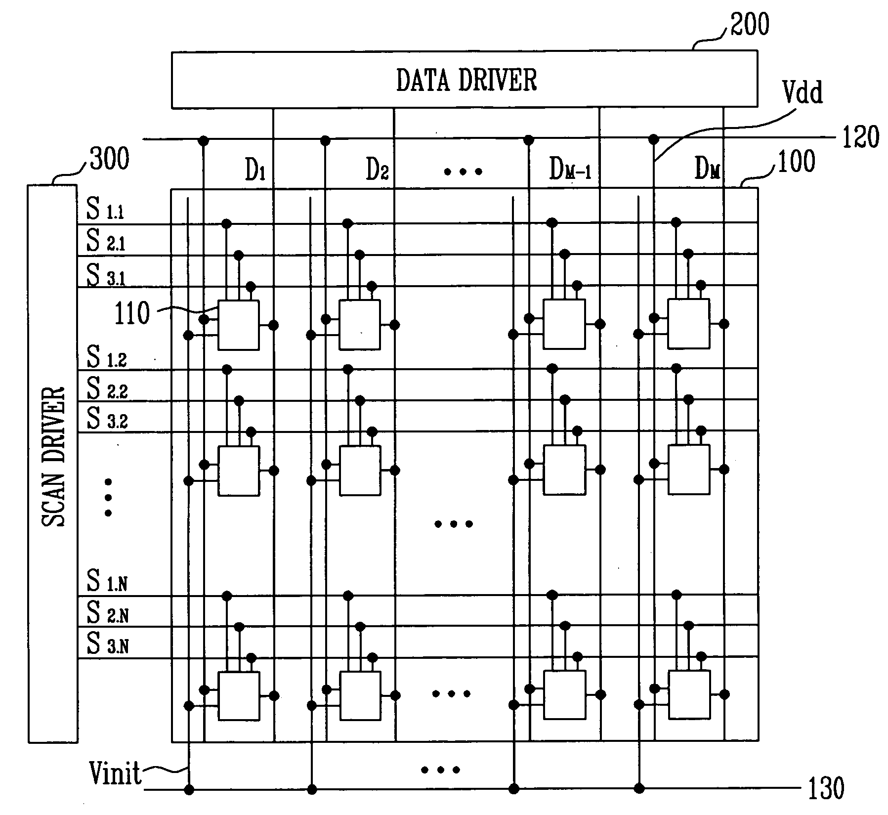
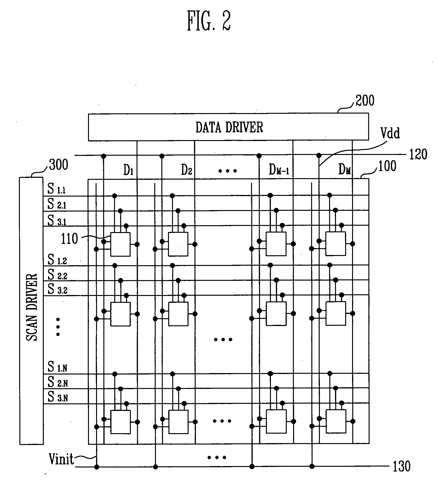
[0031]FIG. 2 illustrates a configuration of a light emitting display according to an embodiment of the present invention. Referring to FIG. 2, the light emitting display comprises a pixel portion 100, a data driver 200, and a scan driver 300. The pixel portion 100 comprises a plurality of pixels 110 including N×M organic light emitting devices; N first scan lines S1.1, S1.2, . . . , S1.N−1, S1.N arranged in a row direction; N second scan lines S2.1, S2.2, . . . , S2.N−1, S2.N arranged in the row direction; N third scan lines S3.1, S3.2, . . . , S3.N−1, S3.N arranged in the row direction; M data lines D1, D2, . . . DM−1, DM arranged in a column direction; M pixel power lines Vdd to supply pixel power; and M compensation power lines Vinit to supply compensation power. Here, each pixel power line Vdd and each compensation power line Vinit are connected to a first power line 130 and a second power line 120.

[0032] Further, a data signal is transmitted from any of the data lines D1, D2, ...


PUM


Abstract

a pixel circuit including a light emitting device; a driving transistor to receive first power and supply current corresponding to voltage applied to a gate electrode thereof to the light emitting device; a first switching device to supply a data signal in response to a first scan signal; a second switching device to supply second power to the gate electrode of the driving transistor in response to the first scan signal; a capacitor to store voltage corresponding to the data signal and the second power according to operations of the first and second switching devices; a third switching device to apply voltage corresponding to the voltage stored in the capacitor to the gate electrode of the driving transistor in response to a second scan signal; and a fourth switching device to transmit the first power to the driving transistor in response to a third scan signal.

Description

CROSS-REFERENCE TO RELATED APPLICATIONS [0001] This application claims the priority of Korean Patent Application No. 2004-80621, filed on Oct. 8, 2004, in the Korean Intellectual Property Office, the entire disclosure of which is incorporated herein by reference. FIELD OF THE INVENTION [0002] The present invention relates to a pixel circuit and a light emitting display comprising the same, and more particularly, to a pixel circuit and a light emitting display comprising the same, in which a threshold voltage is compensated, thereby improving the uniformity of brightness. BACKGROUND [0003] Recently, various flat panel displays have been developed, to substitute cathode ray tube (CRT) displays because the CRT displays are relatively heavy and bulky. Among the flat panel displays, a light emitting display (LED) is notable because it has high emission efficiency, high brightness, wide view angle, and fast response time. [0004] The light emitting display comprises a plurality of light em...

Claims


Application Information

Patent Timeline
IPC IPC(8): G09G5/00H05B44/00
CPCG09G3/3233G09G2300/0819G09G2300/0842G09G2300/0861G09G2310/0251G09G2320/043G09G3/30
Inventor JEONG, JIN TAE
Owner SAMSUNG DISPLAY CO LTD
Why Eureka
Try Eureka