Semiconductor memory device

a memory device and semiconductor technology, applied in semiconductor devices, digital storage, instruments, etc., can solve the problem of inability to improve the operation speed of the dram, and achieve the effect of preventing the shortening of the effective retention time of information and reducing the frequency of refreshing information

Inactive Publication Date: 2006-04-20
KK TOSHIBA
View PDF2 Cites 28 Cited by
  • Summary
  • Abstract
  • Description
  • Claims
  • Application Information

AI Technical Summary

Benefits of technology

[0015] According to this structure, majority carriers stored in the semiconductor layer are not emitted from the semiconductor layer during reading of information. Hence, change of information and shortening of the effective retention time of information can be prevented from occurring. Therefore, it is possible to realize a high-performance semiconductor memory device in which even when the operation speed is increased, the frequency of refreshing information can be reduced, so that the semiconductor memory device can perform a high-speed operation.

Problems solved by technology

As a result, there arises a problem that the operation speed of the DRAM cannot be improved.

Method used


Image

  • Semiconductor memory device
  • Semiconductor memory device
  • Semiconductor memory device

Examples


embodiment 1

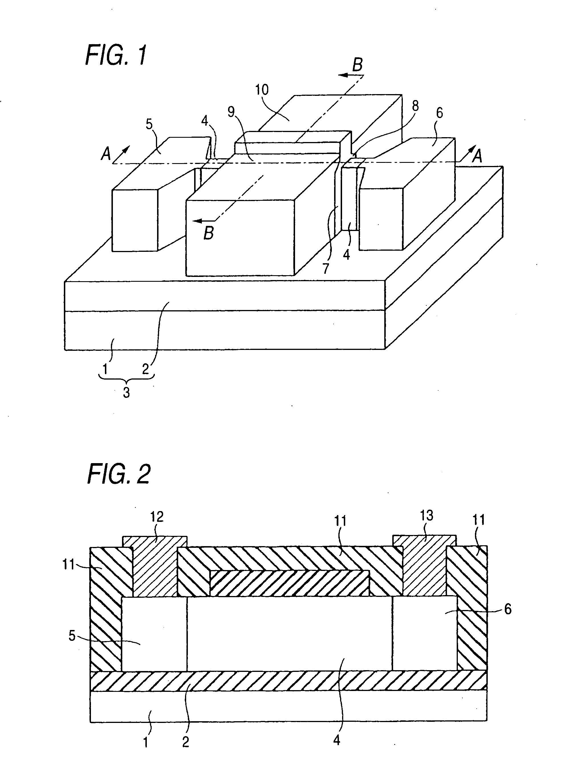
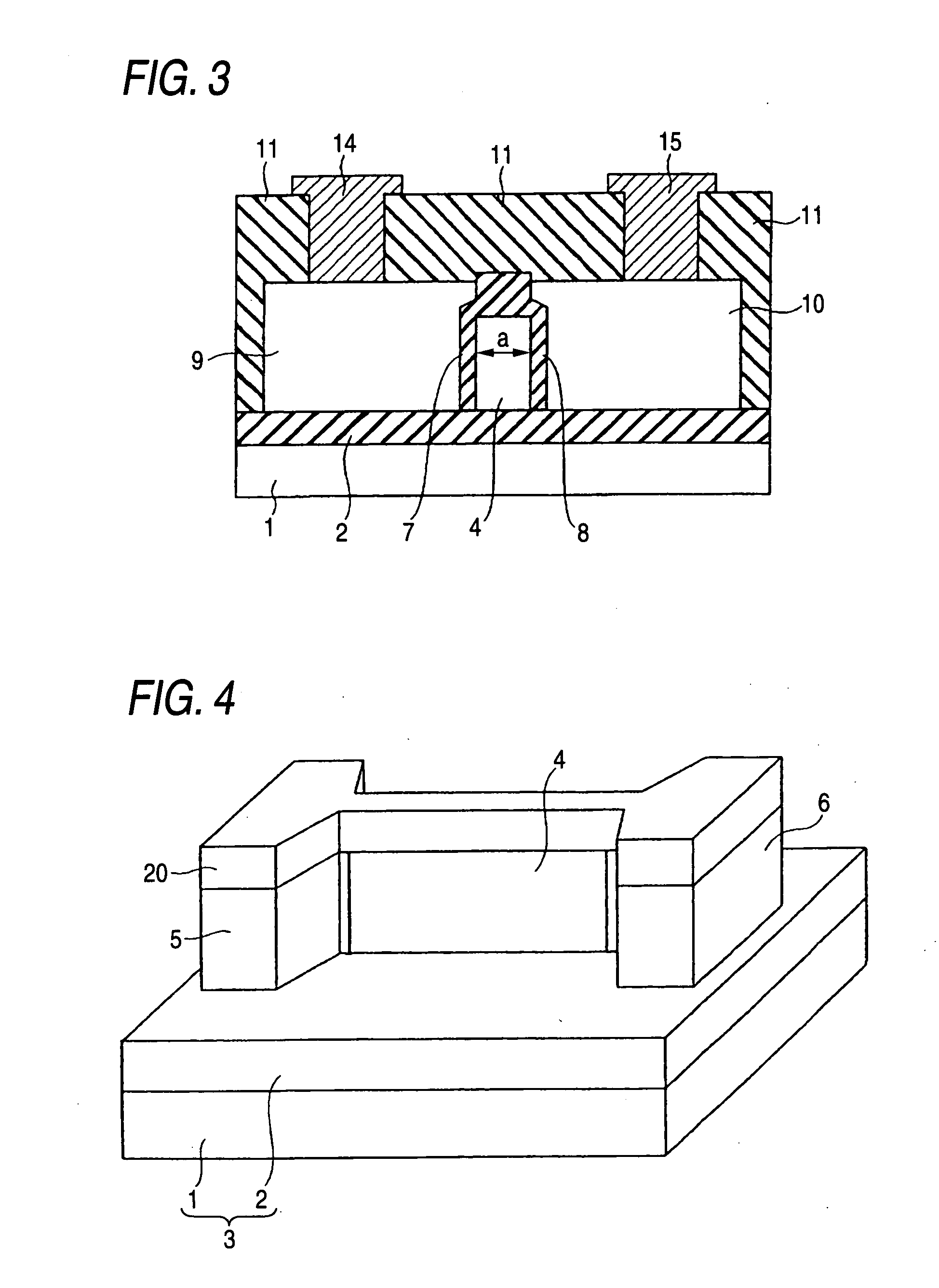
[0030]FIG. 1 is a diagram of a semiconductor memory device of an embodiment 1. FIG. 2 is a section view of the semiconductor memory device of FIG. 1 taken along the line A-A as viewed in the direction of the arrow. FIG. 3 is a section view of the semiconductor memory device of FIG. 1 taken along the line B-B as viewed in the direction of the arrow.

[0031] In FIGS. 2 and 3, an interlayer insulating film and wiring metals are shown. However, in FIG. 1, the interlayer insulating film and wiring metals are omitted in order to facilitate the understanding.

[0032] In the embodiment 1, an n-channel semiconductor memory device will be described as an example. In the case of a p-channel semiconductor memory device, the conductivity type is changed to the opposite conductivity type. In the case of a complementary semiconductor memory device having both the n- and p-channel types, semiconductor memory devices having the same configuration and different conductivity types, tat is, the p- and n-...

embodiment 2

[0065] A second embodiment of the invention will be described with reference to FIG. 7.

[0066] In the semiconductor memory device of the embodiment 2, the source / drain layer 6 is formed only at one end of the channel region 4. This is different from the semiconductor memory device of the embodiment 1, and the other configuration is identical with that of the embodiment 1. The identical components are denoted by the same reference numerals, and their description will be omitted. In the embodiment 2, the source / drain layer 6 may be a source layer or a drain layer.

[0067] The method of fabricating the semiconductor memory device of the embodiment 2 is identical with that of the embodiment 1, and hence its description is omitted.

[0068] Next, the operation of the semiconductor memory device of the embodiment 2 will be described.

[0069] First, the operation of writing information will be described.

[0070] To write information, a voltage is applied to the gate electrodes 9, 10 to cause ca...

embodiment 3

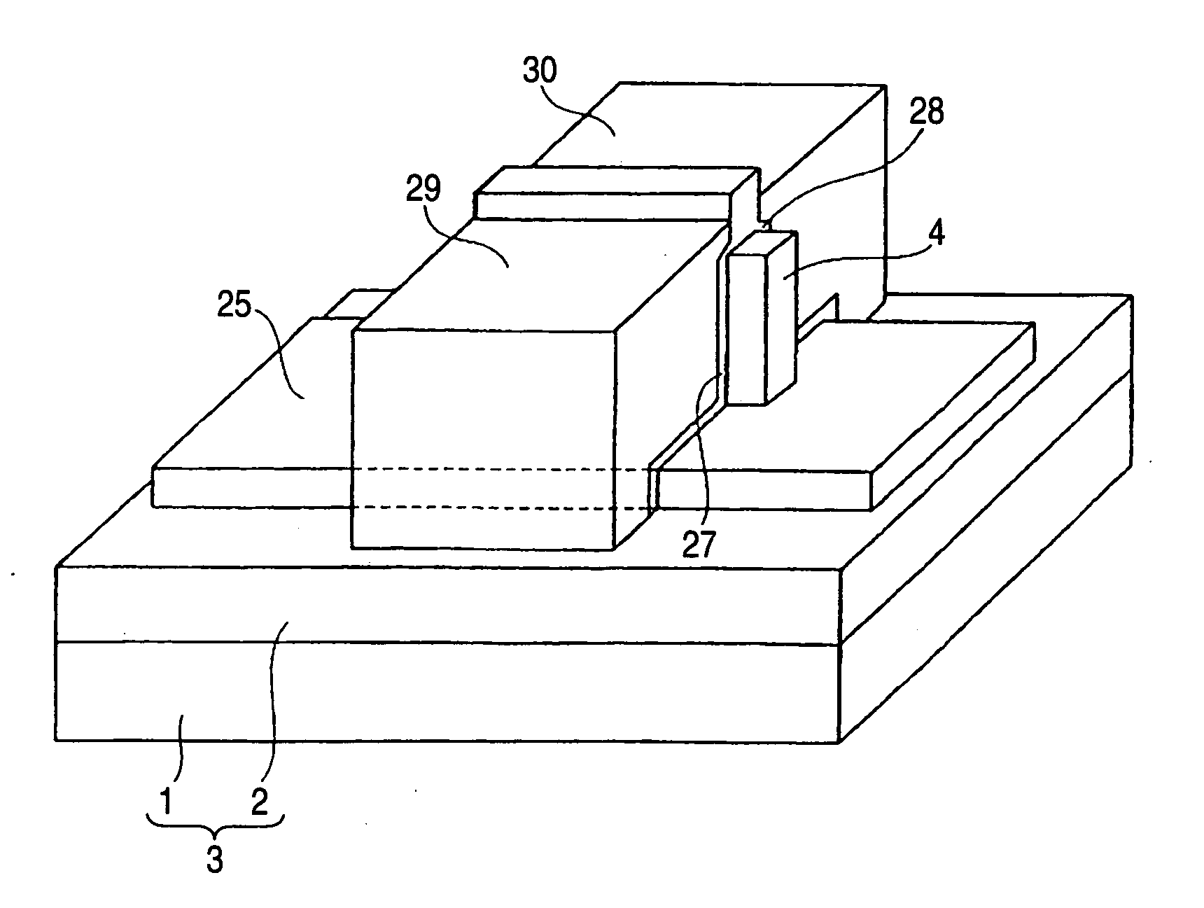
[0075] Next, a third embodiment of the invention will be described with reference to FIG. 8. The semiconductor memory device of the embodiment 3 is different from the semiconductor memory device of the embodiment 1 in that a source / drain layer 25 is not formed at the both ends of the channel region 4, but is disposed below the channel region 4. The other configuration is identical with that of the embodiment 1, the identical components are denoted by the same reference numerals, and their description will be omitted.

[0076] As shown in FIG. 8, in the semiconductor memory device of the embodiment 2, the source / drain layer 25 is disposed on the embedded insulating film 2 of the semiconductor substrate 3, and the channel region 4 is uprightly formed on a middle portion of the upper surface the source / drain layer 25. In other words, the source / drain layer 25 is in contact with an entire bottom surface of the channel region 4.

[0077] A first gate insulating film 27 and a second gate insu...


PUM


Abstract

A semiconductor memory device includes a semiconductor substrate, a semiconductor layer, a source/drain layer, first and second insulating films, and first and second gate electrodes. The semiconductor layer of one conductivity type is formed on a principal surface of the semiconductor substrate. The source/drain layer is formed on the principal surface with being in contact with one end of the semiconductor layer, and has a conductivity type opposite to the one conductivity type. The first insulating film is formed on one side surface of the semiconductor layer. The second insulating film is formed on another side surface of the semiconductor layer. The first gate electrode is formed on the one side surface via the first insulating film. The second gate electrode is formed on the other side surface of the semiconductor layer via the second insulating film, and is opposed to the first gate electrode.

Description

[0001] This application is based upon and claims the benefit of priority from the prior Japanese Patent Application No. 2004-293172 filed on Oct. 6, 2004; the entire contents of which are incorporated herein by reference. BACKGROUND OF THE INVENTION [0002] 1. Field of the Invention [0003] The present invention relates to a semiconductor memory device, and more particularly to a dynamic random access memory. [0004] 2. Description of the Related Art [0005] In a conventional dynamic random access memory (DRAM), a memory cell consists of one field effect transistor and a capacitor. In the field of such a one transistor-one capacitor memory cell, various techniques for reducing the size of the cell have been proposed in order to enhance the integration degree. However, a transistor must be formed vertically, which is technically difficult; there arise problems such as that electrical interference between adjacent memory cells is significant; and there are difficulties in the production t...

Claims


Application Information

Patent Timeline
Patent Type & Authority Applications(United States)
IPC IPC(8): H01L29/04
CPCG11C7/02G11C11/404G11C2211/4016H01L27/108H01L27/10802H01L27/10826H01L29/66795H01L29/7841H01L29/785H01L29/78645H10B12/20H10B12/36H10B12/00
Inventor ONO, MIZUKI
Owner KK TOSHIBA
Why Eureka
Try Eureka