Semiconductor device, semiconductor memory device and data processing system comprising semiconductor system

a semiconductor memory and memory device technology, applied in the field of semiconductor memory devices and data processing systems comprising semiconductor systems, can solve the problems of increasing reducing the data retention time of the memory cell, and increasing the boost voltage required for driving word lines, etc., to achieve excellent operating margin for the sense amplifier, reduce the write voltage of the memory cell, and high speed operation

Active Publication Date: 2011-03-17
PS4 LUXCO SARL
View PDF3 Cites 9 Cited by
  • Summary
  • Abstract
  • Description
  • Claims
  • Application Information

AI Technical Summary

Benefits of technology

[0012]According to the present invention, the write voltage for the memory cell can be reduced, excellent operating margin for the sense amplifier and high-speed operation can be obtained, and it is possible to achieve low power consumption and low cost. Detailed effects will be described below.
[0013]According to the present invention, since the write voltage (third voltage) for the memory cell is set lower than the operation voltage (second voltage) of the sense amplifier and higher than the transfer control voltage of the transfer control circuit, the signal voltage of the bit line obtained by reading the high-level data of the memory cell can be transformed into the operation voltage of the sense node and transferred via the sense node. Accordingly, the operating speed and the sense margin can be ensured in the sense amplifier so that excellent sensing operation is ensured therein, and an effect of reducing the write voltage for the memory cell can be obtained.
[0014]According to the present invention, since the voltage applied to the capacitor of the memory cell can be reduced by reducing the write voltage, the electric field strength condition of a capacitor dielectric film is maintained, reliability of the capacitor dielectric film is maintained and film thickness thereof can be reduced without an increase in the leak current at the data storage node of the memory cell. In this case, since capacitance of the capacitor increases, stored charge amount (Q=CV) of the capacitor can be approximately equal to storage charge amount Q′ in the conventional configuration (in which the write voltage is equal to the operation voltage of the sense amplifier).
[0015]Further, the above structure of the memory cell allows the potential at the P-N junction portion formed between the data storage node of the memory cell and a silicon substrate node to be reduced, the leak current from the memory cell (storage node) to the substrate can be reduced, and data retention time of the memory cell can be prolonged so that an effect of stabilizing the operation of the semiconductor device can be obtained. Further, if the data retention time is prolonged, frequency of refreshing (the number of refreshes per predetermined time) can be reduced, and an effect of reducing consumption current necessary for the refresh operation can be obtained. Further, by reducing the write voltage, the potential of the data storage node corresponding to the high-level data of the memory cell decreases, the boost voltage applied to the gate of the access transistor connected between the capacitor of the memory cell and the bit line when driving the word line. Therefore, in addition to effectiveness of lower power consumption of the semiconductor device, an area for arranging a boost power supply circuit can be reduced, and it is possible to achieve reductions in chip area and cost.

Problems solved by technology

However, the configuration of the above conventional semiconductor memory device is mainly intended to achieve high-speed operation of the sense amplifier, and it is not taken into consideration that a write voltage for the memory cell is set sufficiently lower than an operation voltage of the sense amplifier.
That is, when the write voltage for the memory cell is relatively large, consumption current increases due to charge / discharge current of the bit line.
Further, data retention time of the memory cell is shortened due to influence of leak current from the memory cell (data storage node, exactly) to a substrate, and this causes various problems such as an increase in a boost voltage required for driving word lines.
Thus, there arises a problem that it is difficult for the sense amplifier to normally operate, or a problem that operating speed of the sense amplifier increases even if it operates.

Method used


Image

  • Semiconductor device, semiconductor memory device and data processing system comprising semiconductor system
  • Semiconductor device, semiconductor memory device and data processing system comprising semiconductor system
  • Semiconductor device, semiconductor memory device and data processing system comprising semiconductor system

Examples


Embodiment Construction

[0026]Typical examples of a technical idea solving the problems of the present invention will be shown. However, it goes without saying that the present invention is not limited to the examples of the technical idea and consists in the scope of the claimed invention.

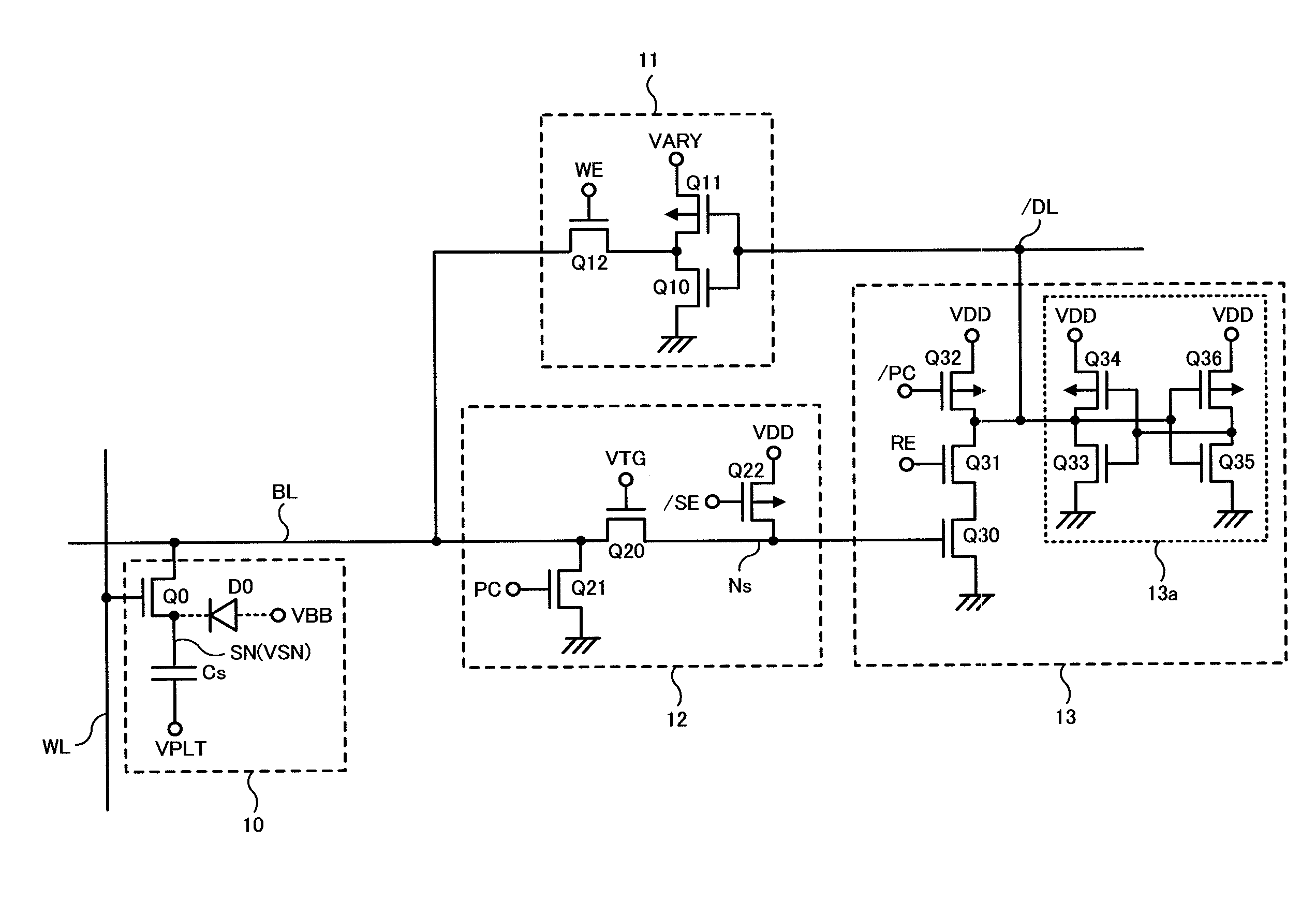
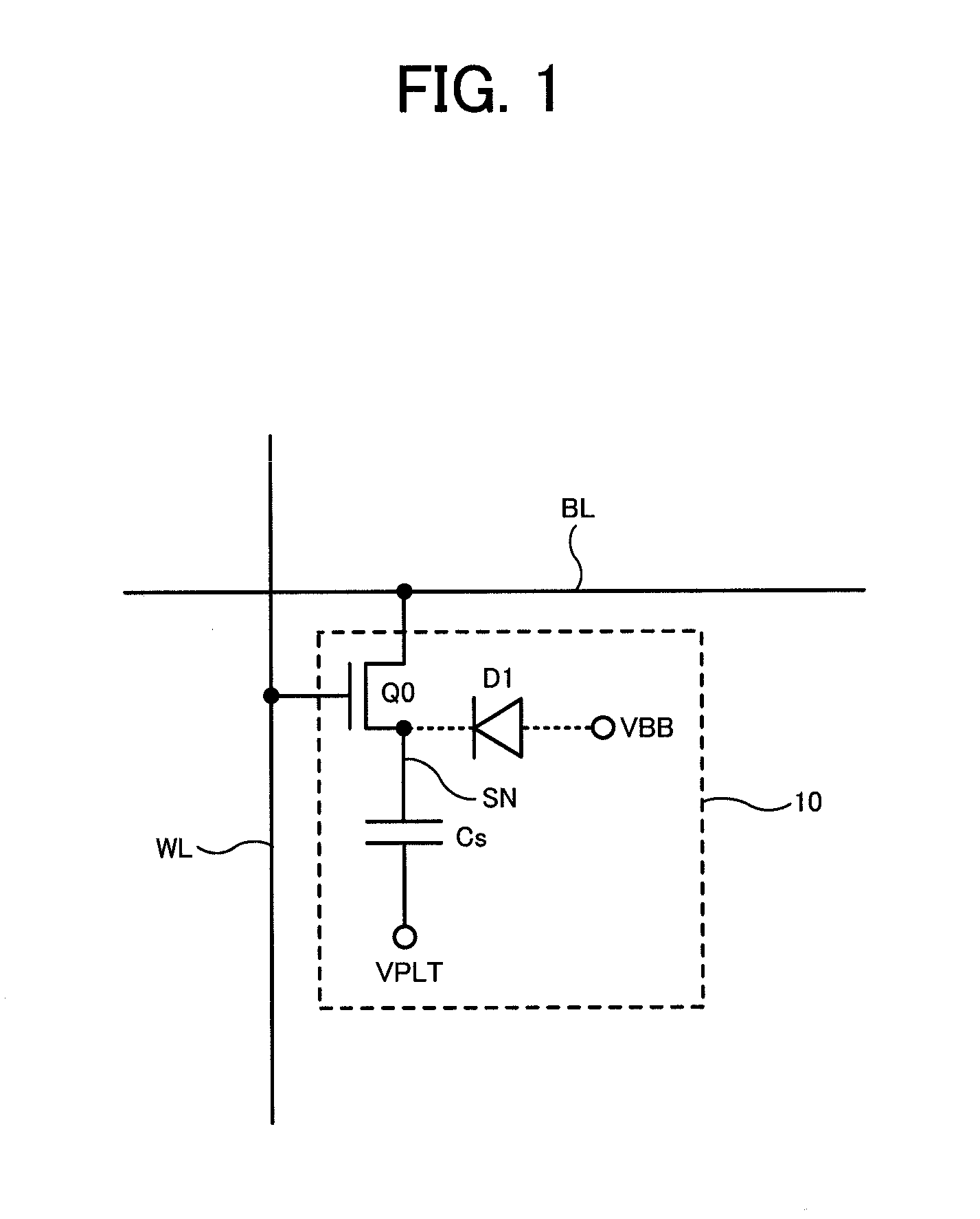
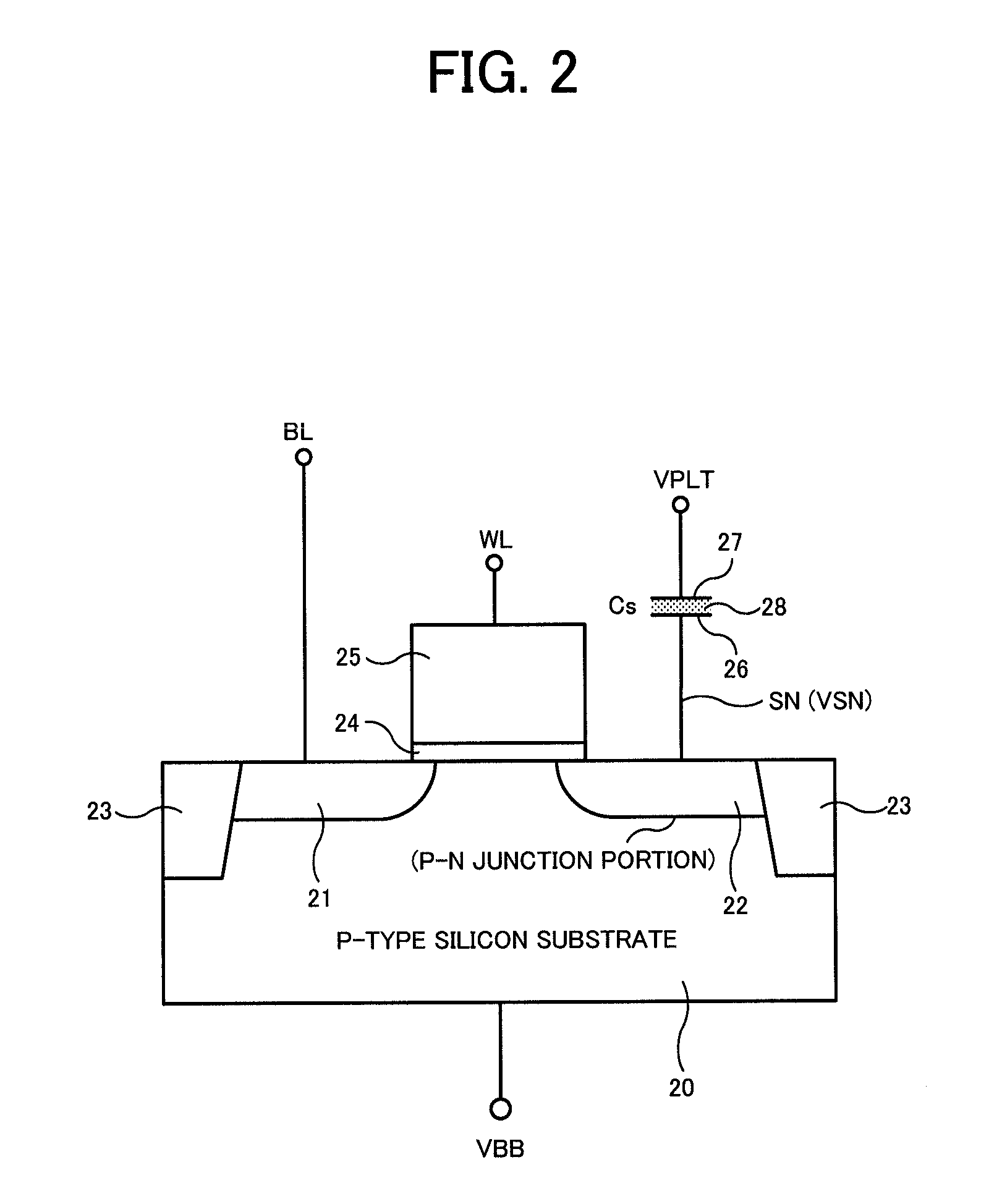
[0027]The technical idea of the present invention is that data (charge amount) of a memory cell (a capacitor) is read out to a bit line, a sense amplifier in which the bit line is connected to a gate of a transistor is configured to amplify the potential of the bit line to an operation voltage of the sense amplifier, a third voltage (VARY) corresponding to high-level data (generally corresponding to “1”) of the memory cell is set lower than a second voltage (VDD) as the operation voltage of the sense amplifier, while the third voltage (VARY) is set higher than a transfer control voltage (VTG) applied to a gate of a transfer transistor (transfer gate) of a transfer control circuit placed between the bit line and the gate ...


PUM


Abstract

A semiconductor device comprises a memory cell, a bit line, a sense amplifier operating between a first voltage and a second voltage higher than the first voltage, a transfer control circuit including a transfer transistor, and a write circuit writing data into the memory cell through the bit line based on the first voltage and a third voltage. The sense amplifier receives and amplifiers the signal voltage at a sense node when the transfer transistor controls the connection between the bit line and the sense node in response to a transfer control voltage. The third voltage is set to a voltage lower than the second voltage and higher than the transfer control voltage, and the sense node is set to a voltage higher than the transfer control voltage in an initial period of a read operation before the data of the memory cell is read out to the bit line.

Description

BACKGROUND OF THE INVENTION[0001]1. Field of the Invention[0002]The present invention relates to a semiconductor device having a configuration in which data stored in memory cells is read out to bit lines and amplified by sense amplifiers.[0003]2. Description of Related Art[0004]Conventionally, semiconductor memory devices each provided with a sense amplifier which senses and amplifies data read out from a memory cell to a bit line have been known (Refer to, for example, Patent References 1 and 2). Further, a memory circuit using a charge transfer amplifier is known in relation to the Patent Reference 1 (Refer to Non-Patent References 1, 2 and 3). Particularly, the Patent Reference 1 discloses a memory cell MC of a gain cell type (a kind of DRAM cells) in which a gate of an output transistor M1 is used as a storage node SN shown in FIG. 8 and description thereof. This memory cell MC stores data in a capacitor (not shown) connected to the storage node SN. Operation of the memory cell...

Claims


Application Information

Patent Timeline
Patent Type & Authority Applications(United States)
IPC IPC(8): G11C11/24G11C7/06
CPCG11C11/4091G11C11/404
Inventor KAJIGAYA, KAZUHIKO
Owner PS4 LUXCO SARL
Why Eureka
Try Eureka