Semiconductor test system

a test system and semiconductor technology, applied in the field of semiconductor test systems, can solve the problems of increasing the price of the semiconductor test device, the burden of high expenses, and the inability to use the semiconductor test device so far used for the test, so as to reduce the effect of reducing the total cost of the facility, and reducing the cost of the test devi

Inactive Publication Date: 2006-04-20
SOCIONEXT INC
View PDF5 Cites 2 Cited by
  • Summary
  • Abstract
  • Description
  • Claims
  • Application Information

AI Technical Summary

Benefits of technology

[0026] According to the present invention, the fail memory for storing fail information and the redundant remedy judging unit for judging based on the fail information as to whether or not a redundant remedy can be made are provided in the redundant remedy judging device independent of the test device which obtains the fail information and connected to the test device via a network, whereby when the capacity of the fail memory is insufficient for larger capacities of semiconductor devices to be tested, the redundant remedy judging device may be replaced with one with the fail memory of a sufficient capacity mounted, and it is not necessary to replace even the test device together with the redundant remedy judging device. Thus, the semiconductor test system according to the present invention is flexibly applicable to semiconductor device of larger capacities, etc. to be tested.
[0027] According to the present invention, when the semiconductor test system, in which the test device and the redundant remedy judging device are independent of each other, is renewed, either alone of the test device and the redu

Problems solved by technology

However, in the test using the conventional semiconductor test device described above, the redundant remedy judging unit of the device is used only in the step of the test before the redundant remedy is made.
That is, the redundant remedy judging unit is unnecessary in the steps of the test after the redundant remedy is made.
This is a cause for increasing the price of the semiconductor test dev

Method used


Image

  • Semiconductor test system
  • Semiconductor test system
  • Semiconductor test system

Examples


second embodiment

A SECOND EMBODIMENT

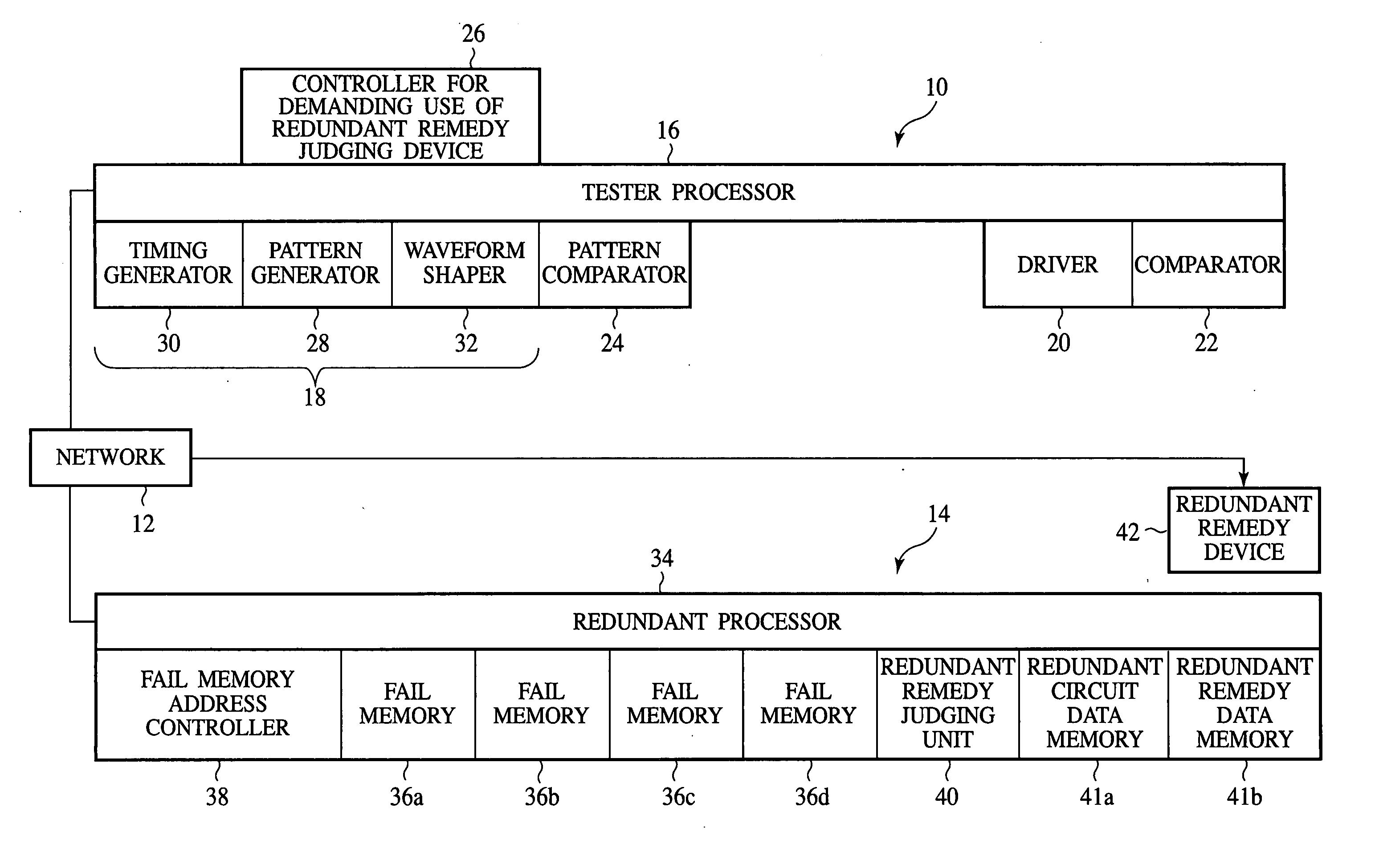
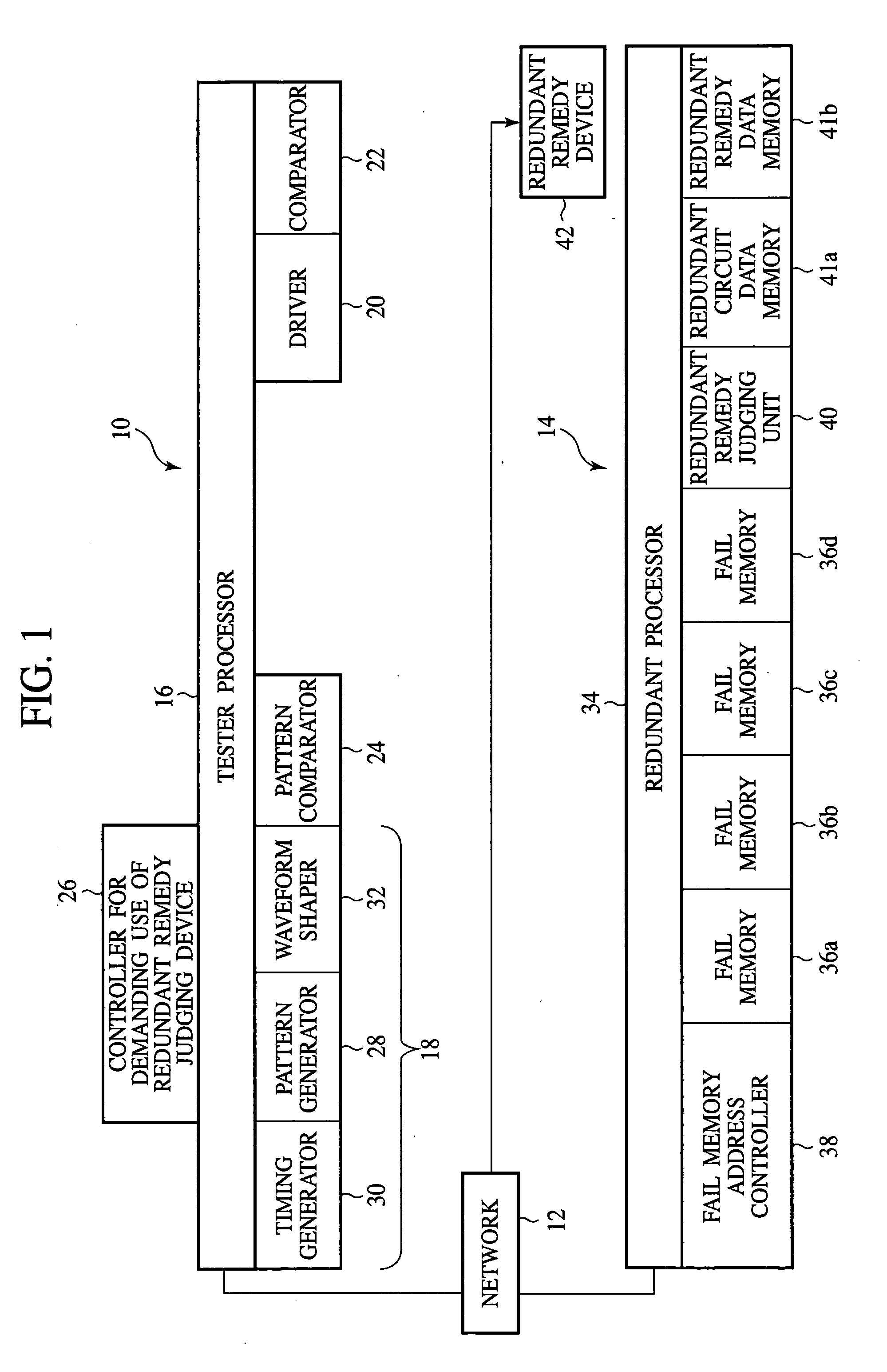
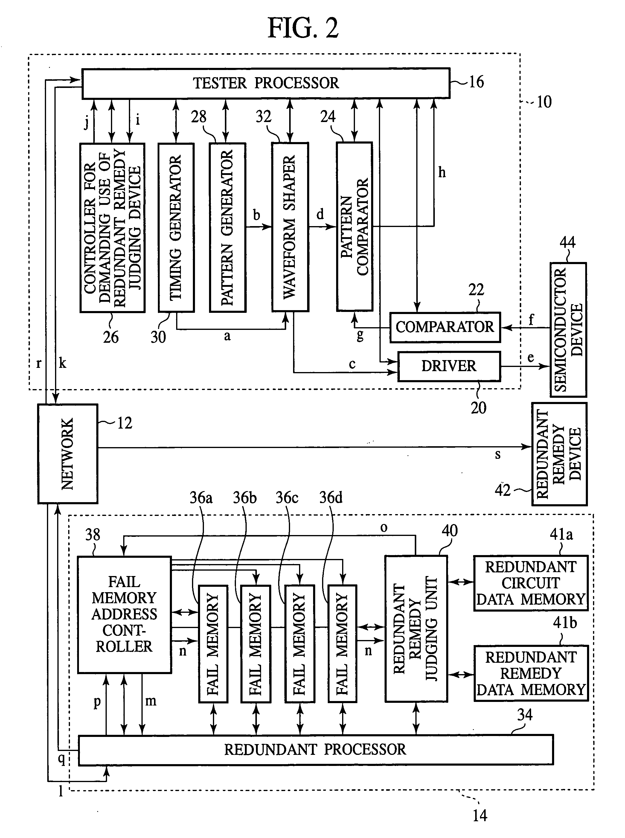
[0086] The semiconductor test system according to a second embodiment of the present invention will be explained with reference to FIG. 3. FIG. 3 is a block diagram of the semiconductor test system according to the present embodiment, which illustrates a constitution thereof. The same members of the present embodiment as those of the semiconductor test system according to the first embodiment are represented by the same reference numbers not to repeat or to simplify their explanation.

[0087] As illustrated in FIG. 3, in the semiconductor test system according to the present embodiment, a plurality of test devices 10 are connected to one redundant remedy judging device 14 via network 12. In FIG. 3, two test devices 10 are connected to one redundant remedy judging device 14 via the network 12. The test devices 10 and the redundant remedy judging device 14 have the same constitutions as those of the semiconductor test system according to the first embodiment.

[0088] ...

third embodiment

A THIRD EMBODIMENT

[0098] The semiconductor test system according to a third embodiment of the present invention will be explained with reference to FIG. 4. FIG. 4 is a block diagram of the semiconductor test system according to the present embodiment, which illustrates a constitution thereof. The same members of the present embodiment as those of the semiconductor test system according to the first and the second embodiments are represented by the same reference numbers not to repeat or to simplify their explanation.

[0099] The basic constitution of the semiconductor test system according to the present embodiment is substantially the same as that of the semiconductor test system according to the second embodiment, in which a plurality of test devices 10 are connected to one redundant remedy judging device 14 via a network 12. In the semiconductor test system according to the present embodiment, each of a plurality of test devices 10 includes a fail memory 46 and a redundant remedy ...


PUM


Abstract

The semiconductor test system comprises a test device 10 for testing semiconductor devices including redundant circuits to obtain fail information of defective parts of the semiconductor devices; a redundant remedy judging device 14 which includes fail memories 36a-36d for storing the fail information, and a redundant remedy judging unit 40 for judging based on the fail information stored in the fail memories 36a-36d as to whether or not the redundant remedy for replacing the defective parts of the semiconductor devices with the redundant circuits can be made, and which is provided independent of the test device 10, wherein the test device 10 and the redundant remedy judging device 14 are interconnected with each other via a network 12, and fail information is transmitted from the test device 10 to the redundant remedy judging device 14.

Description

CROSS-REFERENCE TO RELATED APPLICATIONS [0001] This application is based upon and claims priority of Japanese Patent Application No. 2004-301258, filed on Oct. 15, 2004, the contents being incorporated herein by reference. BACKGROUND OF THE INVENTION [0002] The present invention relates to a semiconductor test system, more specifically a semiconductor test system for use in testing semiconductor devices including redundant circuits. [0003] In a semiconductor memory, such as DRAM or others, generally, redundant circuits, which remedy defects in the memory cell array, are formed. In such a semiconductor device including such redundant circuits, after the operation test is performed, defective parts are remedied by being replaced with the redundant circuits with a laser repair device or others. [0004]FIG. 5 is a diagrammatic view of the conventional semiconductor test device for use in testing semiconductor memories, etc., which illustrates the constitution thereof. [0005] As illustrat...

Claims


Application Information

Patent Timeline
IPC IPC(8): G11C29/00
CPCG11C29/44G11C29/4401G11C29/76
Inventor YANO, TOMOMIOKAMOTO, KOZOMORIMOTO, TAKUMI
Owner SOCIONEXT INC
Why Eureka
Try Eureka