Stacked multiple integrated circuit die package assembly

a technology of integrated circuit dies and package assemblies, which is applied in the direction of electrical equipment, semiconductor devices, semiconductor/solid-state device details, etc., can solve the problems of increased difficulty in connecting input/output bonding pads across several dies, reduced die size for each successive layer, and increased die siz

Inactive Publication Date: 2006-04-27
ETRON TECH INC
View PDF4 Cites 157 Cited by
  • Summary
  • Abstract
  • Description
  • Claims
  • Application Information

AI Technical Summary

Benefits of technology

[0035] Each integrated circuit die on each layer of integrated circuit dies has a size and shape such that, when placed on the integrated circuit dies of a lower layer, each integrated circuit die is offset from edges of the integrated circuit dies of the lower layer. The offset from the edges allows affixing of wirebonds to input/output pads of the integrated circuit dies on t

Problems solved by technology

The drawback of this kind of stacking method is that the size of each die for each successive layer is reduced.
The

Method used


Image

  • Stacked multiple integrated circuit die package assembly
  • Stacked multiple integrated circuit die package assembly
  • Stacked multiple integrated circuit die package assembly

Examples


Embodiment Construction

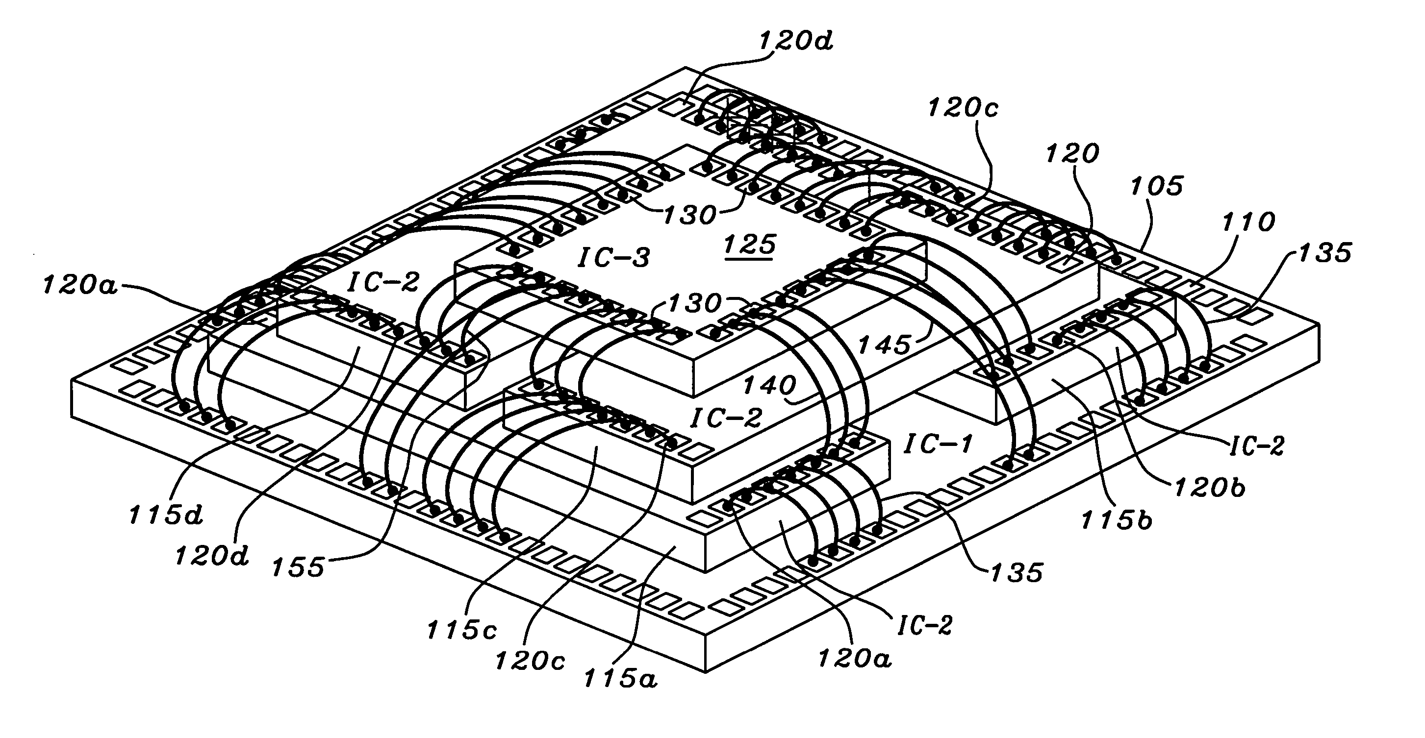
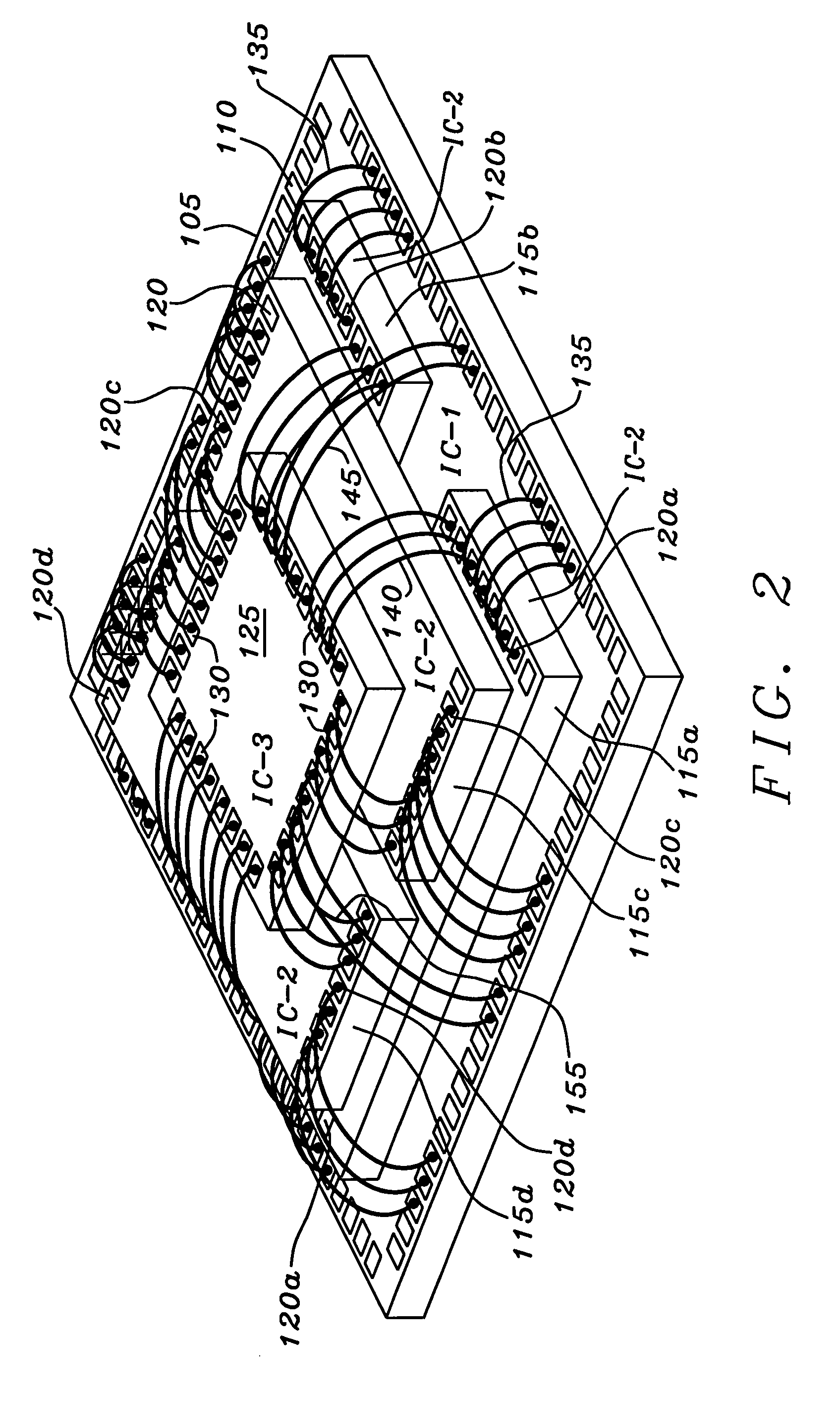
[0041] The electronic package assembly provides multiple integrated circuits dies arranged in a stack. A first layer of the stack is adhered to a substrate such as a printed circuit card, a plastic die carrier, and a ceramic die carrier. Certain layers of the stack contain two or more integrated circuit dies. The sizes and shapes of the integrated circuit dies are selected such that, when the integrated circuit dies are mounted to integrated circuit dies of a lower layer, they are offset from the edges of the integrated circuit dies on the lower layer. The offset distance is chosen such that wirebonds can be attached to the integrated circuit dies of the lower layer.

[0042] The integrated circuit dies on layers with two or more integrated circuit dies have input / output pads placed on two edges of the dies. When two adjacent layers have two or more integrated circuit dies, the integrated circuit dies of each layer are placed orthogonally to permit placement of wirebonds on the integr...


PUM


Abstract

An electronic package assembly is formed with a plurality of integrated circuit dies stacked in layers. At least one first die is placed on a substrate. Each subsequent layer of the stack contains at least one die. Each die on each layer has a size and shape such that, when placed on the dies on a lower layer, it is offset from the edges of the dies on the lower layer to allow affixing of wirebonds to input/output pads of the dies on the lower layer. Each die on each layer with more than one die has input/output pads placed on two sides of the die. Each die on an upper layer is placed orthogonally to each die of a lower each layer such that wirebonds are affixed without interference.

Description

BACKGROUND OF THE INVENTION [0001] 1. Field of the Invention [0002] This invention relates generally to electronic package assemblies and methods. More particularly, this invention relates to three-dimensional electronic package assemblies containing multiple stacked integrated circuit dies. [0003] 2. Description of Related Art [0004] Stacked, or three-dimensional (3D), multiple die packaging methodologies are provide a low-cost, high-volume solution that help system designers reduce the size, weight, and power consumption for small, portable, and wireless consumer devices such as cellular telephone or personal digital assistants. The stacked multiple die packages are commonly referred to as “chip scaled packaging” (CSP). When these packages are used to implement a complete functional system, they are referred to as a system-in-package (SIP). Generally, the SIP includes a computational processor (i.e. a video processor, a digital signal processor, wireless communication controller),...

Claims


Application Information

Patent Timeline
IPC IPC(8): H01L23/02
CPCH01L25/0652H01L25/0657H01L25/18H01L25/50H01L2224/48145H01L2225/06506H01L2225/06527H01L2225/06555H01L2225/06596H01L2924/01079H01L2924/14H01L2924/19041H01L2224/32145H01L2224/49109H01L2224/73265H01L2924/00012H01L2924/10253H01L2924/00H01L24/73
Inventor HSIEH, YUNG-CHING
Owner ETRON TECH INC
Why Eureka
Try Eureka