Method for manufacturing brightness enhancement film of liquid crystal display and structure thereof

a technology of liquid crystal display and brightness enhancement, which is applied in the direction of instruments, polarising elements, transportation and packaging, etc., can solve the problems of insufficient brightness of tft lcd, the choke point of developing tft lcd technology is the brightness, and the solution cannot solve the problem, so as to achieve the effect of manufacturing a plurality of clc films fast and simpl

Inactive Publication Date: 2006-04-27
OPTIMAX TECHNOLOGY CORPORATION
View PDF10 Cites 0 Cited by
  • Summary
  • Abstract
  • Description
  • Claims
  • Application Information

AI Technical Summary

Benefits of technology

[0009] It is an object of the present invention to provide a method for manufacturing a plurality of CLC films fast and simply, i.e. brightness enhancement films.

Problems solved by technology

However, the choke point of developing TFT LCD technology is the brightness.
According to the standard of CRT monitors, the brightness for TFT LCD is not enough.
Although plenty of researches are conducted on the solution to improving brightness, such as increasing luminance of backlight source or LCD, i.e. increasing the aperture ratio of TFT LCD or luminance of all components, most of these solutions can not solve the problem without heat dissipating problem and over-consumption of electricity.
It is a better solution nowadays but the costs are more expensive.
And the relative processes are more complicated.

Method used


Image

  • Method for manufacturing brightness enhancement film of liquid crystal display and structure thereof
  • Method for manufacturing brightness enhancement film of liquid crystal display and structure thereof
  • Method for manufacturing brightness enhancement film of liquid crystal display and structure thereof

Examples


Embodiment Construction

[0046] It is an object of the present invention to provide a method for manufacturing a plurality of CLC films fast and simply, i.e. brightness enhancement films.

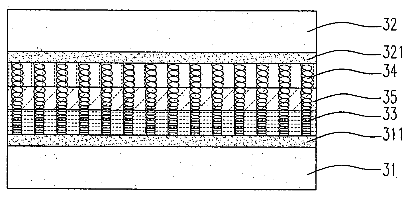
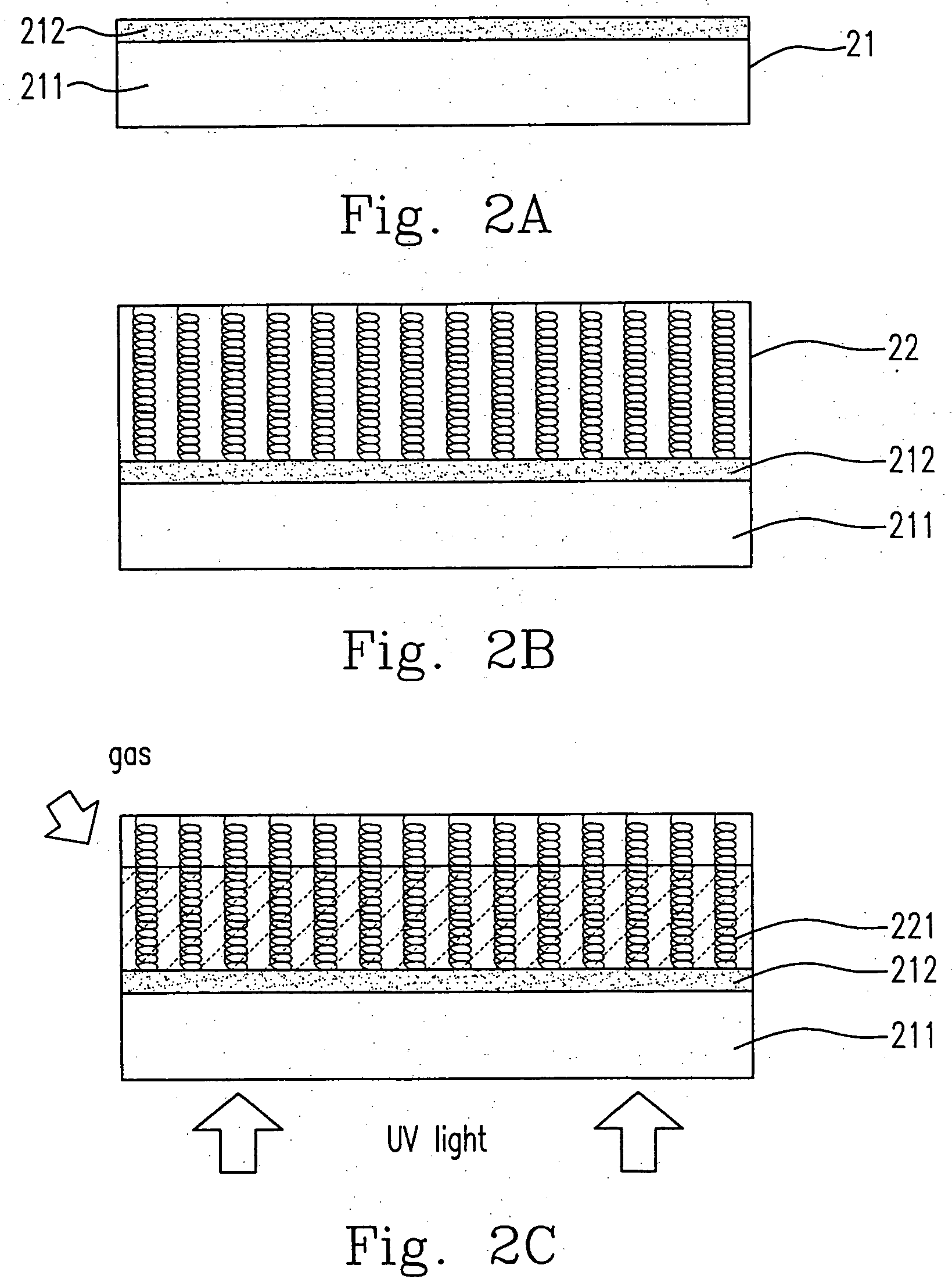
[0047] Please refer to FIG. 2, which is the flowchart showing the method for manufacturing the brightness enhancement film in accordance with the present invention. The manufacturing method includes steps of: (1) providing the first substrate 21, as shown in FIG. 2A; (2) forming the first macromolecule liquid crystal 22 on the first substrate 21 by coating, as shown in FIG. 2B; (3) curing the part of the first macromolecule liquid crystal 22 on the first substrate 21 by UV light which is transmitted through the first substrate 21 so as to form the first light transmitting layer 221, as shown in FIG. 2C; (4) providing the second substrate 23, as shown in FIG. 2D; (5) forming the second macromolecule liquid crystal 24 on the second substrate 23 by coating, as shown in FIG. 2E; (6) curing the part of the second macromolecule ...


PUM

PropertyMeasurementUnit
brightnessaaaaaaaaaa
structureaaaaaaaaaa
luminanceaaaaaaaaaa

Abstract

A brightness enhancement film for use on a display includes a first substrate, a first light transmitting layer mounted on said first substrate, a second light transmitting layer mounted on said first light transmitting layer, a third light transmitting layer mounted between said first light transmitting layer and second light transmitting layer, and a second substrate mounted on said second light transmitting layer, wherein said first and said second light transmitting layer have a first and a second chiral character, respectively, and said third light transmitting layer has a wide-band chiral character.

Description

CROSS REFERENCE TO RELATED APPLICATION [0001] This application is a divisional of U.S. patent application Ser. No. 10 / 761,085, filed Jan. 20, 2004, entitled “Method For Manufacturing Brightness Enhancement Film Of Liquid Crystal Display And Structure Thereof.”BACKGROUND OF THE INVENTION [0002] 1. Field of the Invention [0003] The present invention relates to a manufacturing method for a brightness enhancement film, and more particularly to a manufacturing method for a brightness enhancement film of a liquid crystal display (LCD) and the structure thereof. [0004] 2. Description of Related Art [0005] A backlight module, also known as a backlight unit, is generally an optical assembly providing a backlight source for products and applied to digital camera, PDA (Personal Digital Assistant), GPS (Global Positioning System), medical apparatus, notebook, LCD Monitor, and etc. Owing to the TFT LCD panel itself does not have a light-emitting function, it must have a light source mounted in t...

Claims


Application Information

Patent Timeline
Patent Type & Authority Applications(United States)
IPC IPC(8): C09K19/00B29C35/08G02B5/30G02F1/13357
CPCB29C35/0805B29C2035/0827B29C2791/001B29K2105/0079Y10T428/1036G02B5/3016G02B6/0053G02F1/133606G02F2001/133507B29K2105/243C09K2323/03G02F1/133507
Inventor LI, TUNG LUNGWU, PEI LUNWU, LONG HAI
Owner OPTIMAX TECHNOLOGY CORPORATION
Why Eureka
Try Eureka