Organic light-emitting device array and display

Active Publication Date: 2006-05-04
CANON KK
View PDF35 Cites 17 Cited by
  • Summary
  • Abstract
  • Description
  • Claims
  • Application Information

AI Technical Summary

Benefits of technology

[0011] The present invention can provide an organic light emitting device array which has reduced colo

Problems solved by technology

Then, attention has been paid to the problem that the luminescent color changes between the case where a light emitting device utilizing such technology is viewed from the front and the case where the device is viewed from an obl

Method used


Image

  • Organic light-emitting device array and display
  • Organic light-emitting device array and display
  • Organic light-emitting device array and display

Examples


example 1

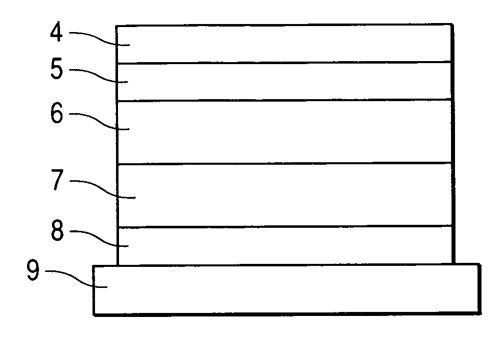
[0069] An organic light emitting device array in accordance with this embodiment has a blue light emitting device, a green light emitting device, and a red light emitting device each having a structure as shown in FIG. 5.

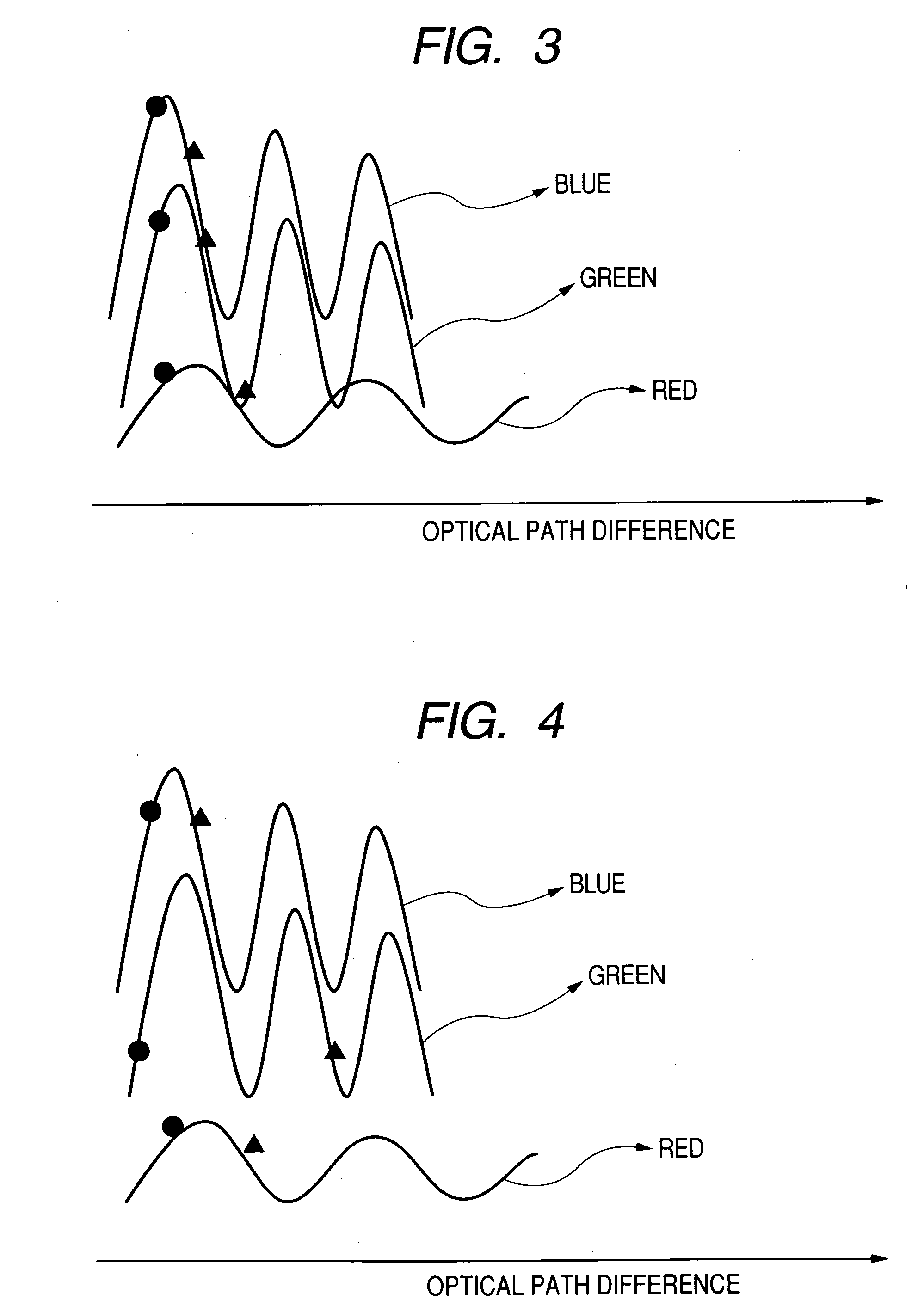
[0070] Further, the optical path difference is set such that the signs of gradients at an optical path difference of 2L of interferograms of the red light emitting device, the green light emitting device, and the blue light emitting device of the organic light emitting device array according to this embodiment are positive. Specifically, an anode 8 is formed of a reflective electrode, a hole transporting layer 7 is constituted of an organic layer with a refractive index n=1.8, and emitted light passes through a transparent cathode 4 to be taken out of the device. Incidentally, the hole transporting layer 7 is formed in a film thickness of 31 nm, and the optical path differences 2L of the red light emitting device, the green light emitting device, and the blue light...

example 2

[0077] An organic light emitting device array in accordance with this embodiment has a red light emitting device, a green light emitting device, and a blue light emitting device each having a structure as shown in FIG. 5.

[0078] Further, the optical path difference is set such that the signs of gradients at an optical path difference of 2L of interferograms of the red light emitting device, the green light emitting device, and the blue light emitting device of the organic light emitting device array according to this embodiment are positive. Specifically, an anode 8 is formed of a reflective electrode, a hole transporting layer 7 is constituted of an organic layer with a refractive index n=1.8, and emitted light passes through a transparent cathode 4 to be taken out of the device. Incidentally, a hole transporting layer 7 of the green light emitting device is formed in a film thickness of 36 nm, a hole transporting layer 7 of the blue light emitting device is formed in a film thickn...


PUM


Abstract

The present invention provides an organic light emitting device array which reduces the change of white balance even if an observation angle is changed. In an organic light emitting device array comprising a plurality of organic light emitting devices which emit lights of different colors, an optical path difference is set such that signs of gradients at an optical path difference of 2L of interferograms for all the plurality of organic light emitting devices are identical to each other.

Description

BACKGROUND OF THE INVENTION [0001] 1. Field of the Invention [0002] The present invention relates to an organic light emitting device array and a display which are capable of full color light emission and white light emission. [0003] 2. Related Background Art [0004] In recent years, development of organic electroluminescence (organic EL; OLED) technology is active. Then, attention has been paid to the problem that the luminescent color changes between the case where a light emitting device utilizing such technology is viewed from the front and the case where the device is viewed from an oblique angle. Japanese Patent Application Laid-Open No. 2002-110363 discloses a device for reducing a spectral change depending on a change of the viewing angle by controlling orientation of a luminescent material. [0005] On the other hand, Japanese Patent-Application Laid-Open No. 2002-367770 discloses a technique for reducing a white color shift while paying attention to that the white color shift...

Claims


Application Information

Patent Timeline
IPC IPC(8): H01L29/08
CPCH01L27/3211H01L51/5281H01L2251/558H10K59/35H10K50/86H10K2102/351
Inventor YUUKI, OSAMUKONDO, SHIGEKIMORII, TOSHIKO
Owner CANON KK
Why Eureka
Try Eureka