Cavity-down Package and Method for Fabricating the same

Inactive Publication Date: 2006-05-04
ADVANCED SEMICON ENG INC
View PDF2 Cites 4 Cited by
  • Summary
  • Abstract
  • Description
  • Claims
  • Application Information

AI Technical Summary

Benefits of technology

[0007] It is therefore an objective of the claimed invention to provide a method for fabricating a cavity-down package, in which the method includes first disposing a chip in the cavity of a chip carrier. Next, a plurality of bonding materials is formed at the corners or edges of the chip and a curing process is performed to cure the bonding materials for protecting the corners or edges of the chip. Next, an encapsulant is formed in the cavity and another curing process is performed to cure the encapsulant. Preferably, the bonding materials can be utilized to protect the corners or edges of the cavity and prevent delamination between the chip and the encapsulant, which results from the expansion and shrinkage phenomenon while the encapsulant is be

Problems solved by technology

Consequently, production yield will greatly decrease and cost of production will increase.
Moreover, when more stru

Method used


Image

  • Cavity-down Package and Method for Fabricating the same
  • Cavity-down Package and Method for Fabricating the same
  • Cavity-down Package and Method for Fabricating the same

Examples


Embodiment Construction

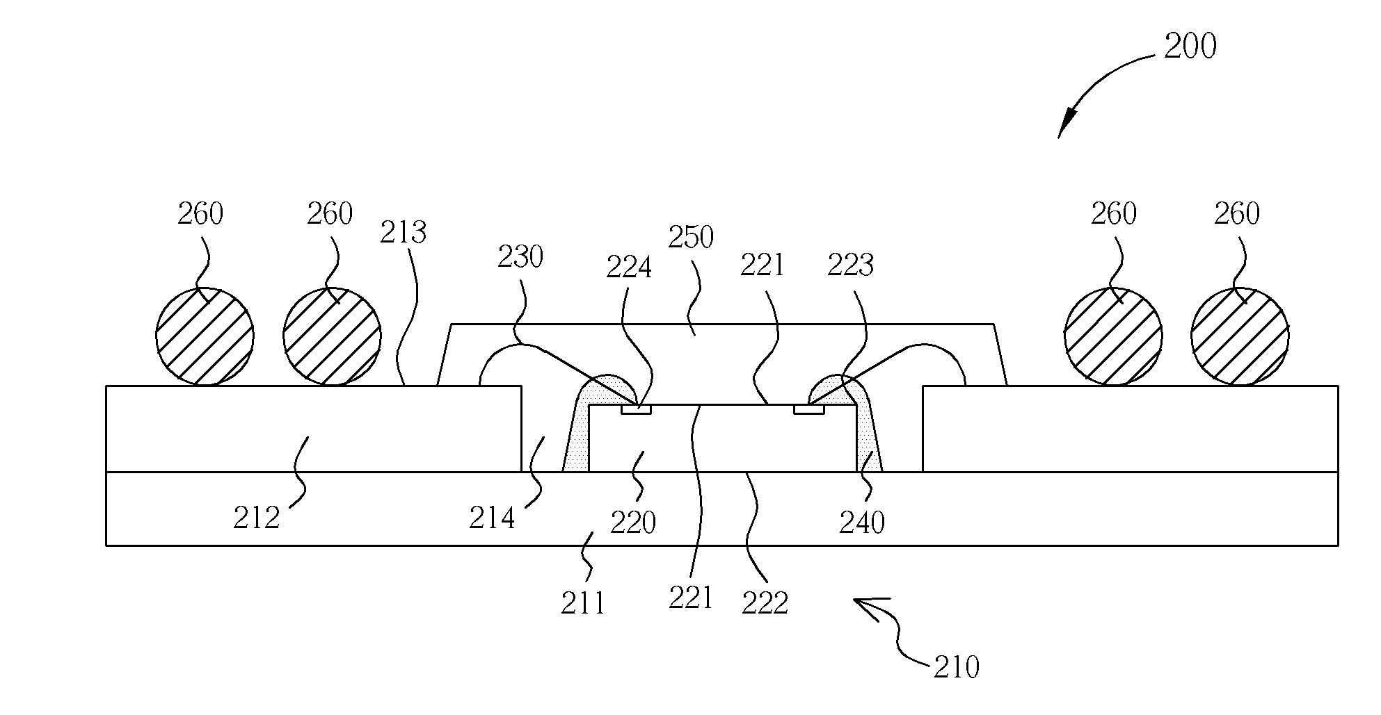
[0015] Please refer to FIG. 3 and FIG. 4. FIG. 3 is a perspective diagram showing the cross-section of a cavity-down package according to the first embodiment of the present invention and FIG. 4a through FIG. 4g are top-view diagrams showing the process of fabricating a cavity-down package according to the first embodiment of the present invention. As shown in FIG. 4a, a chip carrier 210 composed of a heat dissipater 211 and a circuit board 212 is provided, in which the chip carrier 210 includes a surface 213 and a cavity 214 facing the surface 213. Preferably, the surface 213 is an exposed surface of the circuit board 212 for serving as a bonding surface to the outside; and the cavity 214 of the chip carrier 210 is formed by the opening of the circuit board 212 and the heat dissipater 211. Additionally, the heat dissipater 211 is composed of copper or other metals and the circuit board 212 is composed of reinforced fiber including FR-3, FR-4 epoxy or BT resin substrate, polyimide, ...


PUM


Abstract

A method for fabricating a cavity-down package is provided. A chip carrier includes a chip cavity. A chip is disposed inside the cavity, and a plurality of bonding materials is formed at the corners of the chip. The bonding materials are cured to protect the corners of the chip. Next, an encapsulant is formed in the cavity to seal the chip and the bonding materials to prevent stress concentration caused by thermal expansion mismatch on the chip corners and eliminate delamination between the encapsulant and the chip.

Description

BACKGROUND OF THE INVENTION [0001] 1. Field of the Invention [0002] The invention relates to a cavity-down package and method for fabricating the same, and more particularly, to a cavity-down package fabrication method of protecting the corner or edge of a chip before the encapsulating process. [0003] 2. Description of the Prior Art [0004] Cavity-down packages are common packaging forms used in the semiconductor industry. Cavity-down packages have advantages over other forms, such as: better heat dissipation and shorter distance for electrical conductivity. [0005] Please refer to FIG. 1. FIG. 1 is a perspective diagram showing the cross-section of a cavity-down package 100 according to the prior art. As shown in FIG. 1, a chip carrier 110 is composed of a heat dissipater 111 and a circuit board 112 having an opening and a bonding surface 113, in which the opening of the circuit board 112 and the heat dissipater 111 together form a cavity 114 of the chip carrier 110. Additionally, a ...

Claims


Application Information

Patent Timeline
IPC IPC(8): H01L23/28H01L21/52H01L23/13H01L23/31H01L23/36H01L23/498
CPCH01L21/52H01L23/13H01L23/3128H01L23/36H01L23/49816H01L24/48H01L2224/05599H01L2224/48091H01L2224/48227H01L2224/484H01L2224/49175H01L2224/85399H01L2224/8592H01L2924/01029H01L2924/014H01L2924/15153H01L2924/1517H01L2924/15311H01L2924/1532H01L2924/00014H01L24/49H01L2924/01019H01L2924/01033H01L2924/01087H01L2924/00H01L2224/45099H01L2924/15787H01L2924/181H01L2924/00012
Inventor LIN, YU-LIANGHUNG, CHIH-CHENG
Owner ADVANCED SEMICON ENG INC
Why Eureka
Try Eureka