Multilayered chip capacitor array

a multi-layer chip capacitor and array technology, applied in the field of multi-layer chip capacitors, can solve the problems of difficult to increase the number of leads in a limited space to achieve the desired esl reduction effect, and the above structure is unsuitable for use in the conventional multi-layer chip capacitor array

Inactive Publication Date: 2006-05-04
SAMSUNG ELECTRO MECHANICS CO LTD
View PDF8 Cites 16 Cited by
  • Summary
  • Abstract
  • Description
  • Claims
  • Application Information

AI Technical Summary

Benefits of technology

[0012] Accordingly, the present invention has been made keeping in mind the above problems occurring in the prior art, and an object of the present invention is to provide a multilayered chip capacitor array, characterized in that a plurality of capacitors are provided using conductive vias formed in a stacking direction and outer terminals formed on a top surface or a bottom surface of a capacitor body, and the conductive vias are properly disposed, thereby realizing ESL reduction effects.

Problems solved by technology

The conventional multilayered chip capacitor array 10 depicted in FIGS. 1a and 1b includes capacitors arranged in a horizontal direction, and thus, it is difficult to decrease the size thereof when three or more capacitors are used.
However, the above structure is unsuitable for use in the conventional multilayered chip capacitor arrays having a plurality of inner electrodes horizontally arranged.
Thus, it is difficult to increase the number of leads in a limited space to obtain the desired ESL reduction effects.
Further, the conventional multilayered chip capacitor array is disadvantageous because the size thereof cannot decrease due to the structural restriction, and the limitation is imposed on changing the lead structure for ESL reduction.

Method used


Image

  • Multilayered chip capacitor array
  • Multilayered chip capacitor array
  • Multilayered chip capacitor array

Examples


first embodiment

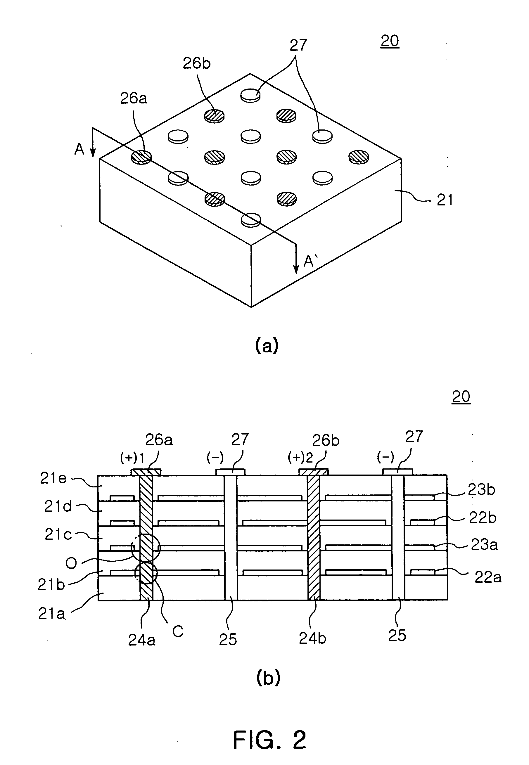
[0034] the connection between the first and second outer terminals 27, 26a and 26b and inner electrodes 22a, 22b, 23a and 23b is realized by vertical conductive vias 25, 24a and 24b as seen in FIG. 2.

[0035]FIG. 2b is a sectional view taken along the line A-A′ in the multilayered chip capacitor array 20 of FIG. 2a.

[0036] As shown in FIG. 2b, the capacitor body 21 of the multilayered chip capacitor array 20 includes a plurality of dielectric layers 21a-21e which are stacked together. The first inner electrodes 23a and 23b and the second inner electrodes 22a and 22b are alternately positioned such that the dielectric layers 21b-21d interpose between the first and second inner electrodes 22a, 23a, 22b and 23b, respectively.

[0037] The first conductive via 25 is connected to the two first inner electrodes 23a and 23b, whereby the first outer terminal 27 is electrically connected with the first inner electrodes 23a and 23b. However, the first conductive via 25 is electrically insulated ...

second embodiment

[0053]FIGS. 5a to 5c are a top plan view and sectional views showing a multilayered chip capacitor array 50 according to the present invention.

[0054] As shown in FIG. 5a, a top surface of a capacitor body 51 is formed with first outer terminals 57 related to negative polarity, second outer terminals 56a related to first positive polarity, and second outer terminals 56b related to second positive polarity. As such, eight first outer terminals 57 are arranged in two rows of one side on the top surface of the capacitor body 51, and the second outer terminals 56a and 56b are divided into groups and four each thereof are arranged in a regular square form in the other two rows.

[0055]FIG. 5b is a sectional view taken along the line B-B′ of FIG. 5a. As shown in FIG. 5b, first conductive vias 55 connected with the first outer terminals 57, and second conductive vias 54a connected with the second outer terminals 56a related to the first positive polarity are connected to first and second inn...

third embodiment

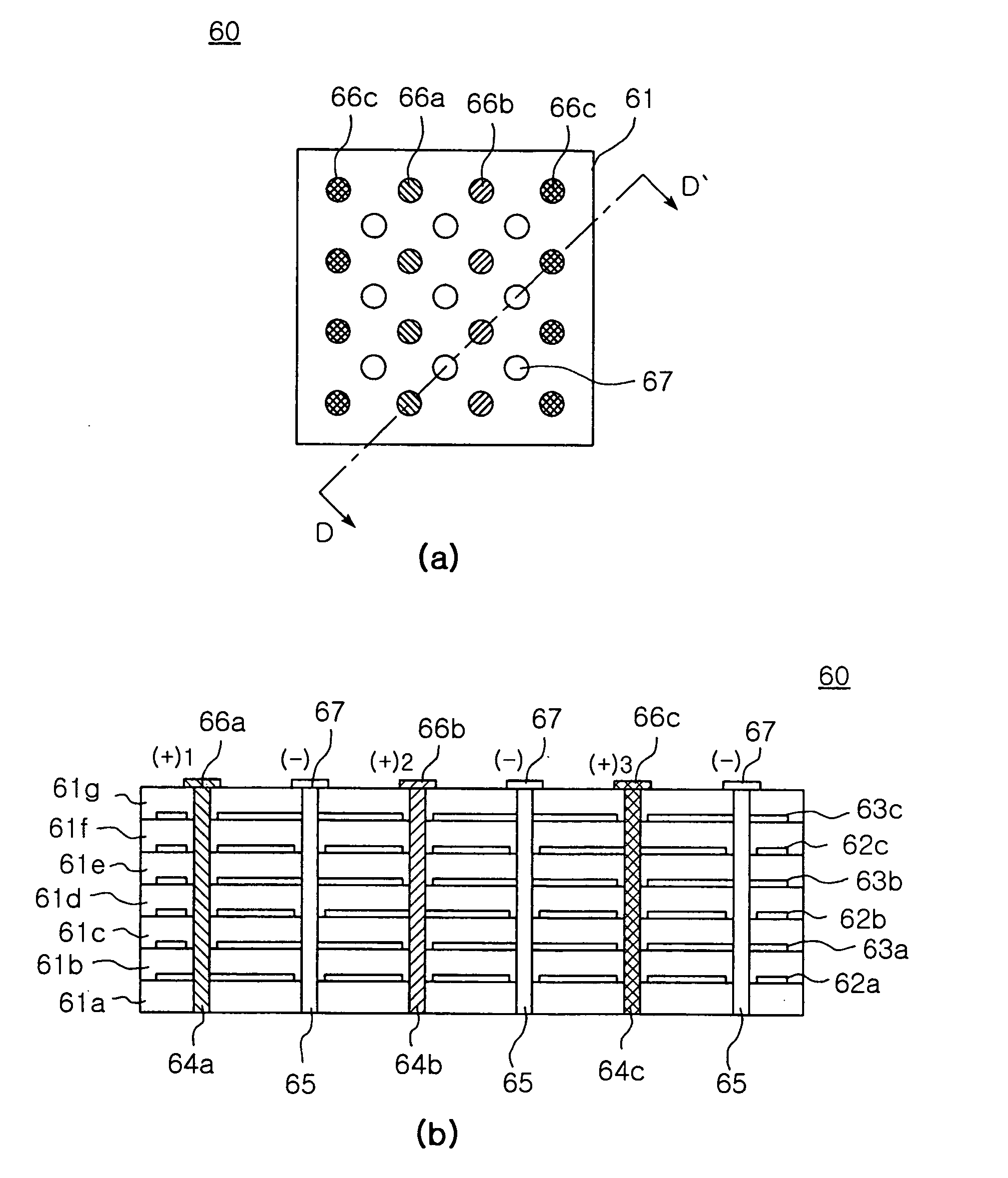
[0062]FIGS. 6a and 6b are a top plan view and a sectional view, respectively, showing a multilayered chip capacitor array 60 having three capacitors according to the present invention. The multilayered chip capacitor array 60 includes three capacitors having a connection structure separately formed only for positive polarity while having a common negative polarity.

[0063] In FIG. 6a, a top surface (or bottom surface) of a capacitor body 61 is formed with first outer terminals 67 related to negative polarity and second outer terminals 66a, 66b and 66c related to positive polarity. The second outer terminal related to positive polarity is divided into second outer terminals 66a, 66b and 66c related to first to third positive polarity.

[0064] As for the outer terminal arrangement according to the third embodiment, the outer terminals of the positive polarity are positioned at corners of a regular square and the outer terminals of the negative polarity are positioned at a central portion...


PUM


Abstract

Disclosed herein is a multilayered chip capacitor array, including a capacitor body having a plurality of dielectric layers, a plurality of pairs of first and second inner electrodes which are formed on the plurality of dielectric layers such that one electrode of one pair of inner electrodes faces the other electrode of the one pair of inner electrodes with one of the plurality of dielectric layers interposed therebetween, at least one first outer terminal and a plurality of second outer terminals formed on at least one surface of a top surface and a bottom surface of the capacitor body, and at least one first conductive via and a plurality of second conductive vias formed in a stacking direction of the capacitor body and connected to the first outer terminal and the second outer terminal, respectively.

Description

BACKGROUND OF THE INVENTION [0001] 1. Field of the Invention [0002] The present invention relates generally to a multilayered chip capacitor, and, more particularly, to a multilayered chip capacitor in which a plurality of capacitors are provided in a single chip. [0003] 2. Description of the Related Art [0004] As well known to those skilled in the art, a multilayered chip capacitor (MLCC) has a structure composed of inner electrodes interposed between a plurality of dielectric layers. The MLCC, which is advantageous because of a small size, a high capacity and easy mounting, is widely applied in various electronic devices. [0005] Recently, to decrease the size of the part and realize an easy mounting process, there is required a multilayered chip capacitor array characterized in that two or more capacitors having the same or different electrostatic capacities are fabricated in a single chip. [0006]FIGS. 1a and 1b are an exploded perspective view and a schematic perspective view, re...

Claims


Application Information

Patent Timeline
Patent Type & Authority Applications(United States)
IPC IPC(8): H01G4/228
CPCH01G2/065H01G4/228H01G4/30H05K1/0231H05K2201/10515H05K2201/1053H01L2224/0554H01L2224/05568H01L2224/05573H01L2224/06131H01L2224/16235H01L2924/00014H01L2924/15159H01L2924/19041H01L2924/19106H01L2224/05599H01L2224/0555H01L2224/0556
Inventor HWA LEE, BYOUNGSATO, HIROKISHIM, CHANG HOONPARK, SANG SOOCHUNG, HAE SUKPARK, DONG SEOKPARK, MIN CHEOLYI, HYUN JUKWON, MIN KYOUNGHAN, SEUNG HEON
Owner SAMSUNG ELECTRO MECHANICS CO LTD
Why Eureka
Try Eureka