Check patentability & draft patents in minutes with Patsnap Eureka AI!

Magneto-resistive RAM having multi-bit cell array structure

a cell array and magnetoresistive ram technology, applied in the field of magnetoresistive rams, can solve problems such as difficulty in accurately applying a desired amount of magnetic field

Active Publication Date: 2006-05-04
SAMSUNG ELECTRONICS CO LTD
View PDF6 Cites 12 Cited by
  • Summary
  • Abstract
  • Description
  • Claims
  • Application Information

AI Technical Summary

Benefits of technology

[0030] According to an embodiment of the present invention, a magnetic RAM includes an access transistor formed on a substrate, first and second resistance-variable elements, and current supplying lines.
[0031] The first and second resistance-variable elements are formed on the access transistor, and the first and second resistance-variable elements are electrically connected to each other. A bit line is formed on the second resistance-variable element. The current supplying lines are respectively disposed between neighboring two of the access transistor and the first and second resistance-variable elements. The first resistance-variable element has different resistance characteristics from the second resistance-variable element.
[0032] According to an embodiment of the present invention, a magnetic RAM capable of simultaneously writing or reading n-bit data, includes an access transisto

Problems solved by technology

Furthermore, during a write operation, it is difficult to accurately apply a desired amount of magnetic field by adjusting the magnitude and direction of the current.

Method used


Image

  • Magneto-resistive RAM having multi-bit cell array structure
  • Magneto-resistive RAM having multi-bit cell array structure
  • Magneto-resistive RAM having multi-bit cell array structure

Examples


Embodiment Construction

[0052] Hereinafter, embodiments of the present invention will be described in detail with reference to the appended drawings. Like reference numbers refer to like components throughout the drawings.

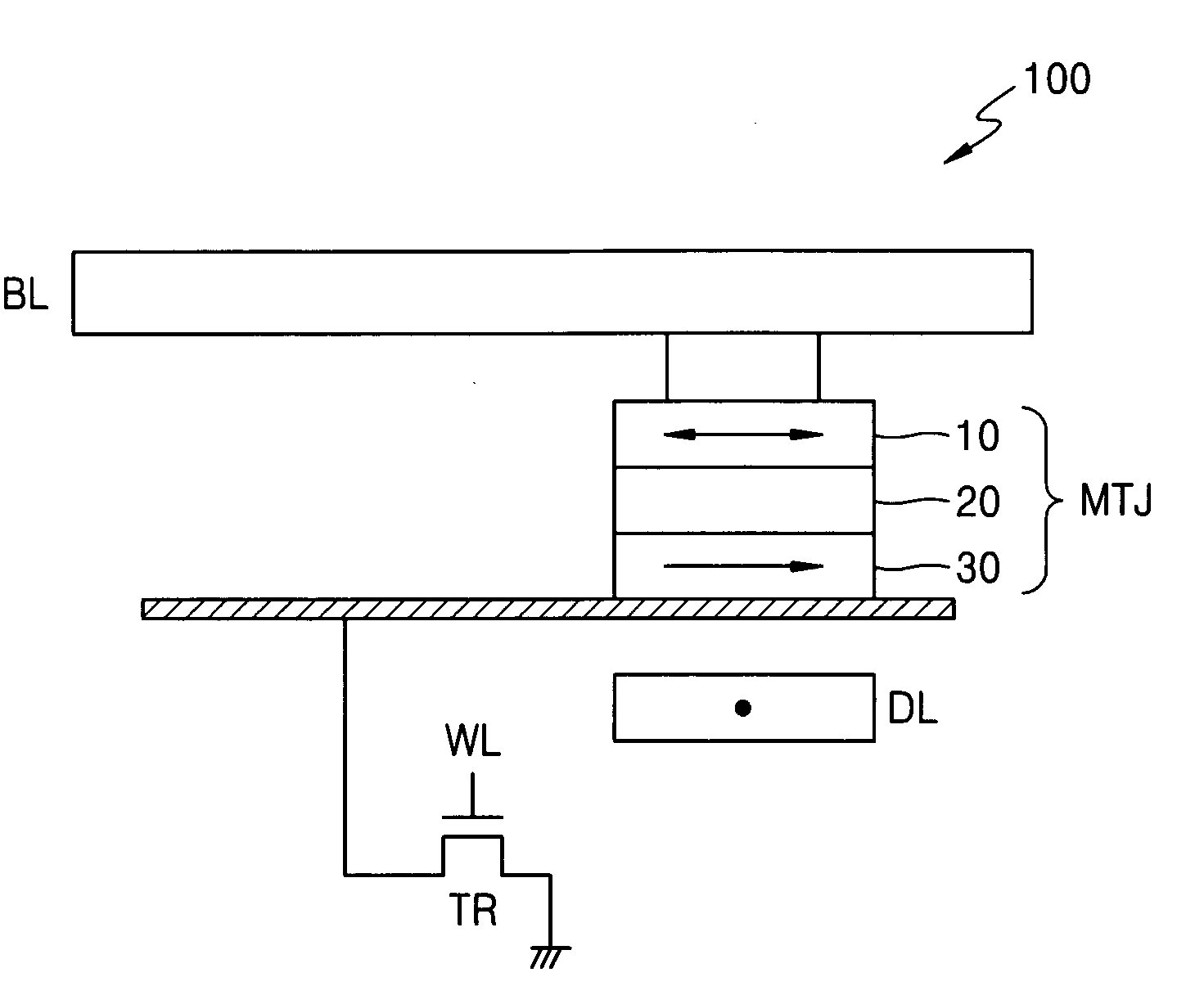
[0053]FIG. 3A is a schematic view of a magnetic RAM 300 according to an embodiment of the present invention.

[0054]FIG. 3B is a perspective view of a second current supplying line CSL2 of the magnetic RAM 300 of FIG. 3A.

[0055] Referring to FIG. 3A, to generate a magnetic field during a data write operation, first through third current supplying lines CSL1, CSL2, and CSL3 are disposed, respectively, between a first resistance-variable element MTJ1 and a second resistance-variable element MTJ2, between the second resistance-variable element MTJ2 and a third resistance-variable element MTJ3, and between the third resistance-variable element MTJ3 and an access transistor TR. The first through third resistance-variable elements MTJ1, MTJ2, and MTJ3 are disposed between the access transistor ...


PUM


Abstract

A magnetic random access memory (RAM) with a multi-bit cell array structure includes an access transistor formed on a substrate, first through third resistance-variable elements, and first through third current supplying lines. The first through third resistance-variable elements are disposed between a bit line and the access transistor, and electrically connected to each other. The first through third current supplying lines are stacked alternately with the first through third resistance-variable elements. The first through third resistance-variable elements have equal resistances.

Description

[0001] This application claims the priority of Korean Patent Application No. 10-2004-0086556, filed on Oct. 28, 2004, in the Korean Intellectual Property Office, the disclosure of which is incorporated herein in its entirety by reference. BACKGROUND OF THE INVENTION [0002] 1. Field of the Invention [0003] The present invention relates to a magneto-resistive RAM, and more particularly, to a magneto-resistive RAM having a multi-bit cell array structure. [0004] 2. Description of Related Art [0005] A magnetic RAM (Random Access Memory) device implements a plurality of resistance-variable components connected to a transistor. Such a magnetic RAM is a memory device, which writes information by changing the directions of magnetization of the respective ferromagnetic thin films and reads information by sensing a change in current caused by the change in the directions of the respective ferromagnetic thin films. Magnetic RAM is a non-volatile and can achieve high-speed operation, low power c...

Claims


Application Information

Patent Timeline
IPC IPC(8): G11C11/00
CPCB82Y10/00G11C11/15G11C11/16G11C11/5607G11C2211/5615H01L27/228H03L7/0812H03L7/0891G11C11/1659G11C11/1673G11C11/1675G11C11/1653G11C11/1693H10B61/22H01L27/105
Inventor KIM, HYE-JINCHO, WOO-YEONGOH, HYUNG-ROK
Owner SAMSUNG ELECTRONICS CO LTD
Features
  • R&D
  • Intellectual Property
  • Life Sciences
  • Materials
  • Tech Scout
  • Unparalleled Data Quality
  • Higher Quality Content
  • 60% Fewer Hallucinations
Learn More