Phase change memory device and method of operating the same

a phase change memory and memory device technology, applied in the direction of static storage, digital storage, instruments, etc., can solve the problems of reducing the lifetime of flash memory, affecting the reliability of conventional phase change memory devices, etc., to achieve high reliability and high integrity

Active Publication Date: 2006-05-04
SAMSUNG ELECTRONICS CO LTD
View PDF3 Cites 33 Cited by
  • Summary
  • Abstract
  • Description
  • Claims
  • Application Information

AI Technical Summary

Benefits of technology

[0015] Embodiments of the present disclosure may provide a phase change memory device with high reliability and high integrity.

Problems solved by technology

However, when flash memory devices are repeatedly used, insulating characteristics of the insulator for tunneling deteriorate.
As a result, the lifetime of a flash memory decreases.
Therefore, a conventional phase change memory device cannot be easily integrated due to the difficulty in reducing the size of the access transistor 10.

Method used


Image

  • Phase change memory device and method of operating the same
  • Phase change memory device and method of operating the same
  • Phase change memory device and method of operating the same

Examples


Embodiment Construction

[0036] Embodiments of the present invention will now be described more fully with reference to the accompanying drawings, in which exemplary embodiments of the disclosure are shown. The invention may, however, be embodied in many different forms and should not be construed as being limited to the embodiments set forth herein. In the drawings, elements are exaggerated for clarity.

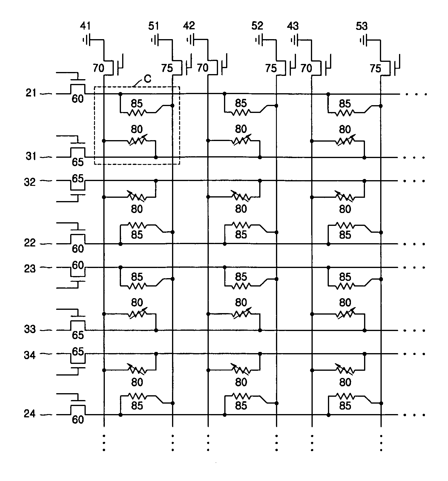
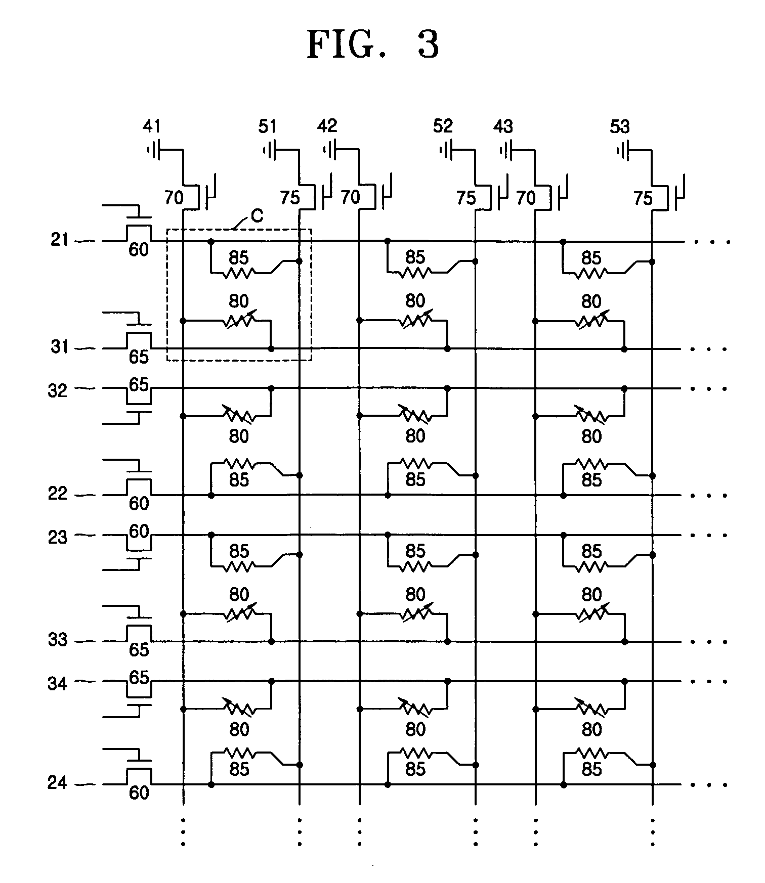
[0037]FIG. 3 is an equivalent circuit diagram of a portion of a cell array of a phase change memory device according to an embodiment of the present disclosure.

[0038] Referring to FIG. 3, the cell array may include a plurality of unit cells C arranged in a matrix composed of rows and columns; a plurality of program bit lines 21, 22, 23, and 24 and a plurality of read bit lines 31, 32, 33 and 34 extending along rows; and a plurality of read word lines 41, 42 and 43 and a plurality of program word lines 51, 52 and 53 extending along columns.

[0039] In this case, the number of the unit cells C, and the number...


PUM


Abstract

A phase change memory device and a method of operating the same are provided. The phase change memory device may include a plurality of unit cells arranged in a matrix composed of rows and columns; a plurality of program bit lines and read bit lines arranged in rows, each of the program and read bit lines having a row selection transistor formed at one end thereof; and a plurality of program word lines and read word lines arranged in columns, each of the program and read word lines having a column selection transistor formed at one end thereof. Each of the unit cells may include a phase change resistor and an exothermal resistor used to heat the phase change resistor.

Description

BACKGROUND OF THE DISCLOSURE [0001] This application claims the benefit of Korean Patent Application No. 10-2004-0086539, filed on Oct. 28, 2004, in the Korean Intellectual Property Office, the disclosure of which is incorporated herein in its entirety by reference. 1. FIELD OF THE DISCLOSURE [0002] Embodiments of the present disclosure may include a non-volatile semiconductor memory device, and more particularly, a phase change memory device and a method of operating the same. 2. DESCRIPTION OF THE RELATED ART [0003] Semiconductor memory devices are categorized into volatile memory devices and non-volatile memory (NVM) devices. Volatile memory devices, such as DRAMs, are used in, for example, computers to store and process data in a short time when power is supplied. [0004] However, as demand for mobile phones and digital cameras increases, the demand for non-volatile memory devices increases due to their advantages over DRAMs. For example, non-volatile devices can process data in ...

Claims


Application Information

Patent Timeline
Patent Type & Authority Applications(United States)
IPC IPC(8): G11C11/00
CPCG11C8/08G11C13/0004G11C13/0028G11C13/0069G11C2013/008
Inventor CHOI, SANG-JUNLEE, JUNG-HYUNMA, DONG-JOONPARK, WAN-JUNPARK, YOUNG-SOO
Owner SAMSUNG ELECTRONICS CO LTD
Why Eureka
Try Eureka