Semiconductor device

a semiconductor device and semiconductor technology, applied in semiconductor devices, semiconductor/solid-state device details, electrical equipment, etc., can solve the problems of difficult suppression of contact between the bonding wire and the second chip, the cost of processing is extra, and the cost of reduction is difficult to meet the requirements of the second chip, etc., to achieve high-quality semiconductor devices and high-quality semiconductors

Inactive Publication Date: 2006-05-11
NEC ELECTRONICS CORP
View PDF9 Cites 7 Cited by
  • Summary
  • Abstract
  • Description
  • Claims
  • Application Information

AI Technical Summary

Benefits of technology

[0013] According to the present invention, the average grain size of the filler contained in the adhesive layer between the first element and the second element is relatively larger than a distance between adjacent wires connected to the first element. For this reason, contact between the first element and the second element can be suppressed, and the filler can be suppressed from passing through a gap between the wires. Therefore, a high-quality semiconductor device can be provided.
[0014] According to the present invention, the first and second elements can be suppressed from being in contact with each other, and the filler can be suppressed from passing through a gap between the wires, so that a high-quality semiconductor device is provided.

Problems solved by technology

However, these spacer structures were the obstructions of the cost reduction because material cost of the spacer is excessively high and cost of processing is extra necessary.
However, when an adhesive agent containing a spacer filler is used to assure a clearance of a bonding wire, it is difficult to suppress contact between the bonding wire and a second chip.
In this case, since the adhesive agent 5 containing the spacer filler is necessary to keep viscosity thereof and physical characteristics thereof after hardening desired value, it is difficult to make the filler content extremely high.
Therefore a circuit forming surface of the first chip 2 may be damaged.

Method used


Image

  • Semiconductor device
  • Semiconductor device
  • Semiconductor device

Examples


first embodiment

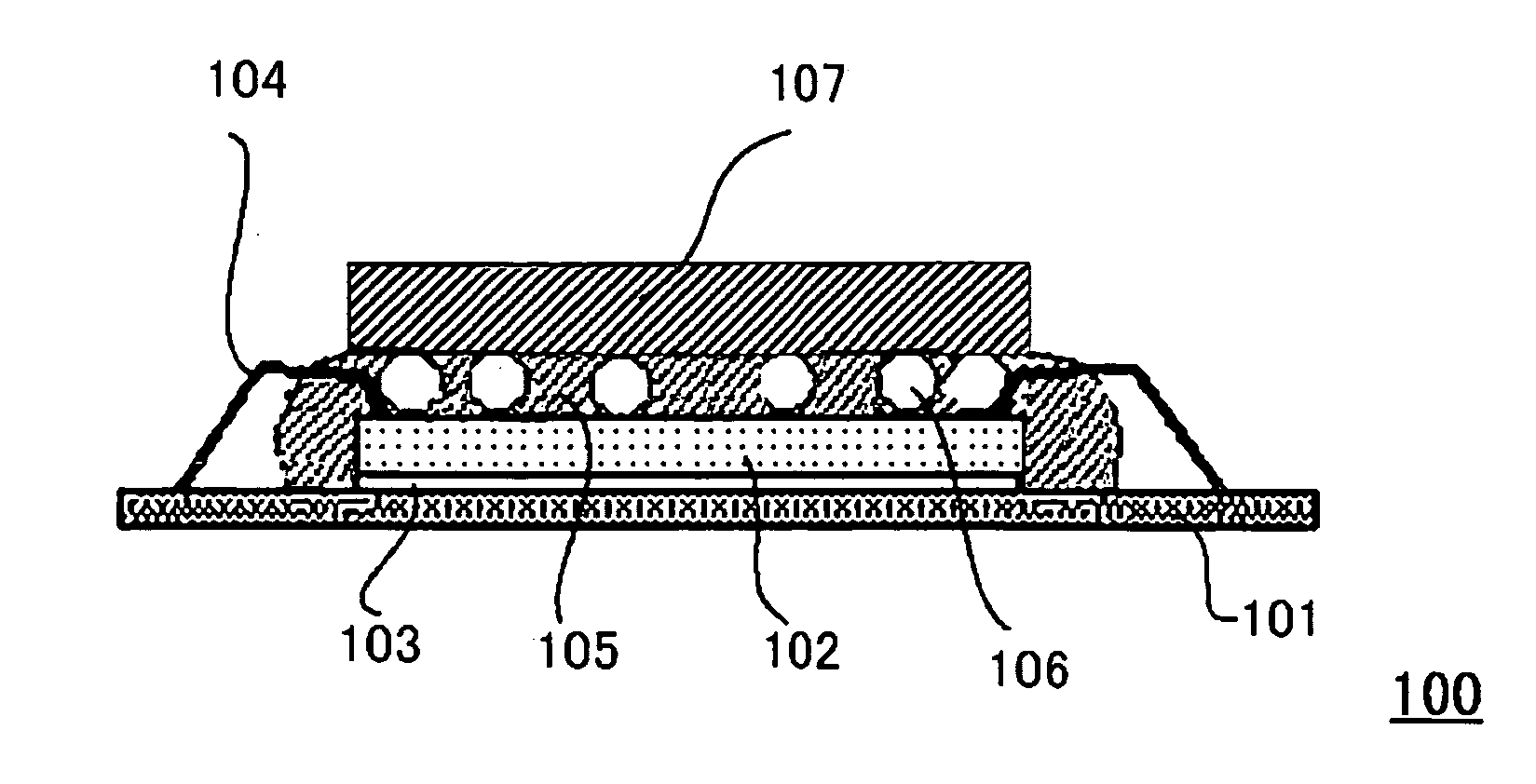
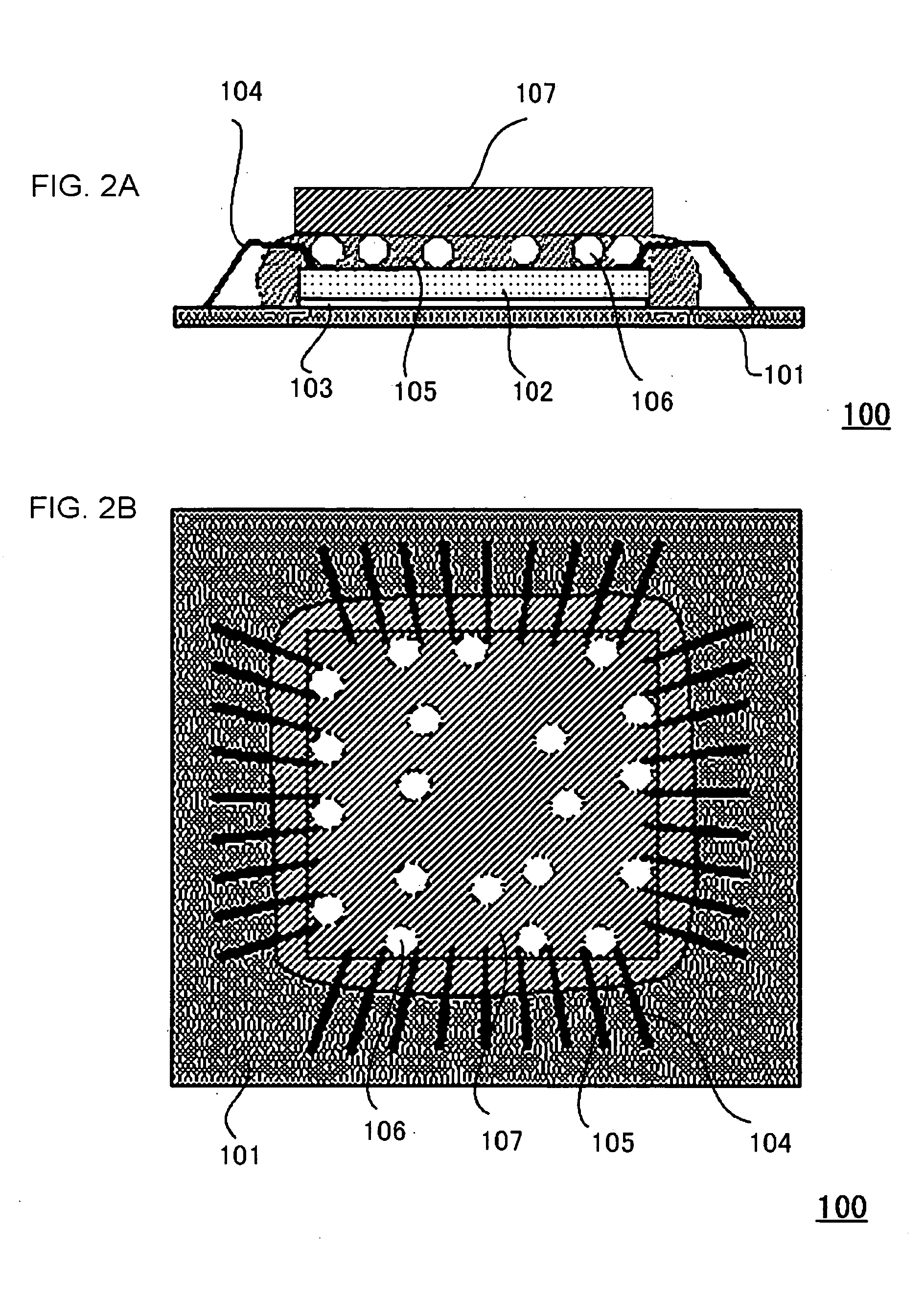
[0024] A semiconductor device shown in FIGS. 1A and 1B and FIGS. 2A and 2B includes an interconnect substrate 101 serving as a substrate on which bonding pads are formed, a first chip 102 serving as a first element having a plurality of pads as electrodes stacked on the interconnect substrate 101, and a second chip 107 serving as a second element stacked on the first chip 102. The bonding pads formed on the interconnect substrate 101 are connected to the first chip 102 by bonding using wires 104. The second chip 107 is located immediately above at least some of the plurality of pads formed on the first chip 102. An adhesive layer containing a filler 106 is formed between the first chip 102 and the second chip 107. An average grain size of the filler 106 is larger than a distance between the adjacent wires 104 formed on the first chip 102.

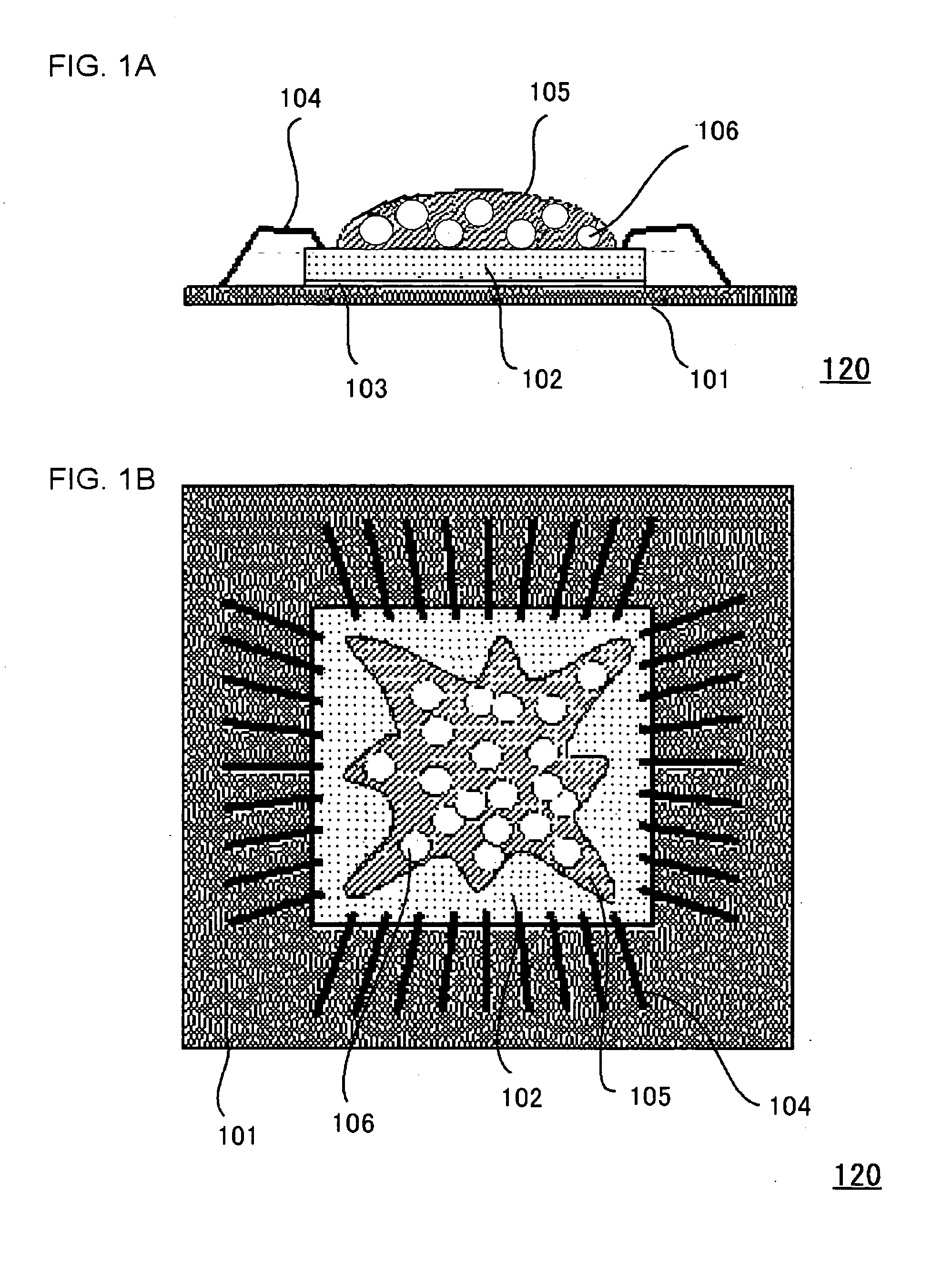
[0025]FIGS. 1A and 1B show a semiconductor device 120 to which an adhesive agent is applied according to the embodiment of the present invention, ...

second embodiment

[0045] A semiconductor device which will be described in this embodiment uses a sheet-like adhesive agent as an adhesive agent 105. The sheet-like adhesive agent is stuck on the lower surface of a second chip 107 in advance and cause a first chip 102 to adhere to the second chip 107 by a heating / pressure-bonding method. The present embodiment is different from the first embodiment in these points.

[0046]FIGS. 3A and 3B show a semiconductor device 130, and FIGS. 4A and 4B show a semiconductor device 140 on which the second chip 107 according to the embodiment is mounted.

[0047] In the semiconductor device 130 according to the embodiment, as shown in FIG. 3A, a sheet-like adhesive agent 112 is stuck on a rear surface (lower surface) of the second chip 107 in advance.

[0048] The sheet-like adhesive agent 112 contains a filler 106. The average grain size of the filler 106 is 80 μm as in the fist embodiment. As a base material mainly constituting the sheet-like adhesive agent 112, a B-st...


PUM


Abstract

In a semiconductor device, an average grain size of a filler contained in an adhesive agent applied to the first chip is larger than an interval between adjacent wires. When the second chip is pressed downward, the filler is caught between the wires, a larger number of filler grains is held between the first and second chip. The interval between the first and the second chip can be stably maintained. Since the number of filler grains left to be held between the first and second chip is larger than that in the conventional art, a pressure applied to the second chip is uniformly distributed while suppressing the number of filler grains contained in the adhesive agent from increasing, and a pressure applied to the grains is lower than that in the conventional art.

Description

[0001] This application is based on Japanese Patent application NO. 2004-326270, the content of which is incorporated hereinto by reference. BACKGROUND [0002] 1. Technical Field [0003] The present invention relates to a chip-stack-type semiconductor device. [0004] 2. Related Art [0005] In a chip-stack-type semiconductor device on which a first chip and a second chip are sequentially stacked, the sizes of these chips may approximate to each other, or the size of the second chip may be larger than the size of the first chip. In these cases, since the second chip is located above a bonding wire for connecting the first chip and a substrate, it must be considered that the bonding wire is not in contact with the second semiconductor chip. For this reason, a semiconductor device having a spacer structure in which a dummy chip or an elastomer having a size slightly smaller than the first chip is sandwiched between the first chip and the second chip to keep insulation by assuring a clearanc...

Claims


Application Information

Patent Timeline
Patent Type & Authority Applications(United States)
IPC IPC(8): H01L23/29
CPCH01L24/29H01L24/33H01L25/0657H01L25/16H01L2224/32225H01L2224/48227H01L2224/73207H01L2224/73265H01L2224/83191H01L2225/0651H01L2225/06575H01L2924/01029H01L2924/01079H01L2924/14H01L2924/19041H01L2224/29H01L2224/2919H01L2924/01005H01L2924/01006H01L2924/01033H01L2924/014H01L2924/0665H01L2224/29101H01L2924/00H01L2924/00013H01L2224/29099H01L2224/29199H01L2224/83139H01L2224/32145H01L2924/00012H01L2224/29299H01L2224/2929H01L2924/00014H01L2224/49171H01L24/73
Inventor SHIRONOUCHI, TOSHIAKIKISHIDA, FUMIAKI
Owner NEC ELECTRONICS CORP
Why Eureka
Try Eureka