Non-volatile semiconductor memory device and method for reading the same

a non-volatile semiconductor and memory device technology, applied in static storage, digital storage, instruments, etc., can solve the problems of difficult to set the read reference ir to be a desired value, and the inability to achieve the optimum read conditions, etc., to achieve stably read out, high accuracy, and high accuracy.

Active Publication Date: 2006-05-11
CETUS TECH INC
View PDF3 Cites 14 Cited by
  • Summary
  • Abstract
  • Description
  • Claims
  • Application Information

AI Technical Summary

Benefits of technology

[0035] According to the present invention, a read reference can be set with high accuracy and data can be read out with high accuracy. Specifically, by setting a read reference to be a preferable value, an error does not occur during a read operation even under strict conditions, whereby data can be stably read out. Further, a significant difference is obtained between a read current and the read reference, resulting in a high-speed read operation and a low-voltage read operation. Furthermore, test conditions in a manufacturing process can be relaxed, thereby making it possible to improve the yield of a non-volatile semiconductor memory device and reduce cost.
[0036] According to the first and second aspects of the present invention, a read reference can be set with high accuracy by using a reference current used for erase verification and write verification without setting a read reference during a test before shipment, and data can be read out with high accuracy. According to the third to sixth aspects of the present invention, the state of a reference cell is set based on a memory cell current. Therefore, even when there are variations during a manufacturing process or a change in characteristics during an operation, a read reference can be set with high accuracy and data can be read out with high accuracy. Particularly, according to the fourth aspect of the present invention, a similar effect can be obtained for a multi-valued non-volatile semiconductor memory device. According to the seventh aspect of the present invention, a read reference is set on a block-by-block basis where the block is small, thereby making it possible to further improve the accuracy of setting the read reference. According to the eighth aspect of the present invention, methods of setting a read reference are switched, so that a portion of a non-volatile semiconductor memory device can be used as a binary or more memory, while the remaining portion can be used as a four- or more-valued memory.

Problems solved by technology

However, it is difficult to set the read reference IR to be a desired value with high accuracy using any of these methods.
Therefore, optimum read conditions are not necessarily obtained when an average value of memory cell currents in the states is used as a read reference.

Method used


Image

  • Non-volatile semiconductor memory device and method for reading the same
  • Non-volatile semiconductor memory device and method for reading the same
  • Non-volatile semiconductor memory device and method for reading the same

Examples


first embodiment

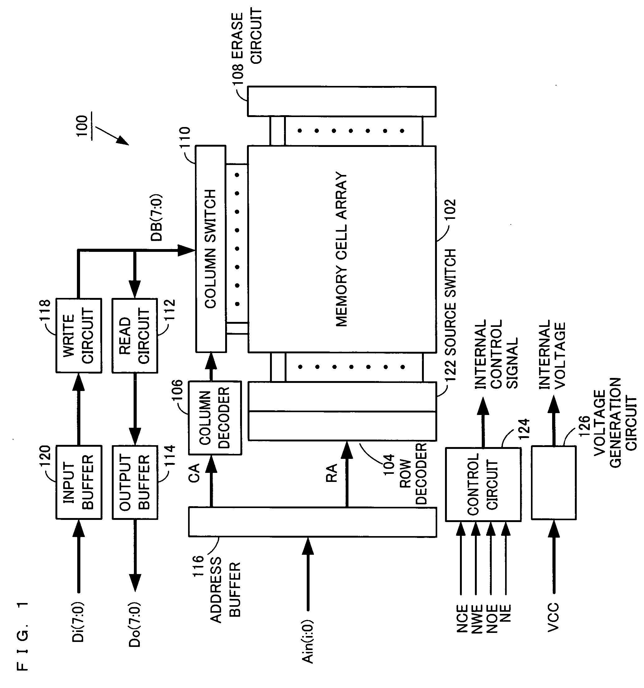
[0069]FIG. 1 is a diagram illustrating a structure of a flash EEPROM according to a first embodiment of the present invention.

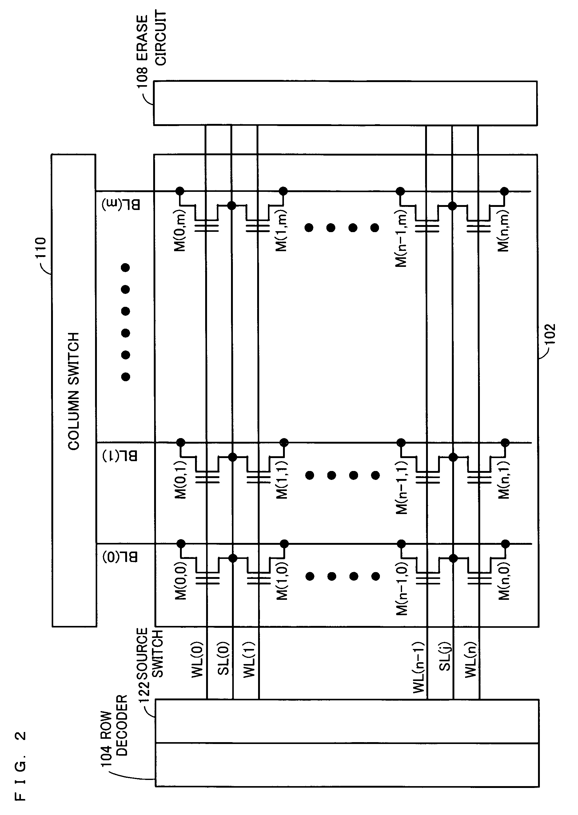
[0070]FIG. 2 is a diagram illustrating details of a memory cell array contained in the flash EEPROM of FIG. 1. In this and other embodiments, it is assumed that input / output data has a bit width of 8 bits in flash EEPROMs described below.

[0071] A flash EEPROM 100 of FIG. 1 comprises a memory cell array 102 for storing data. In the memory cell array 102, memory cell transistors M(0, 0) to M(n, m) having a double-gate structure are provided on corresponding intersections of word lines WL(0) to WL(n) and bit lines BL(0) to BL(m) (see FIG. 2). The control gates of memory cells provided on the same row are connected in common to a corresponding one of the word lines WL(0) to WL(n). The drains of memory cells provided on the same column are connected in common to a corresponding one of the bit lines BL(0) to BL(m). Two opposing sources of a pair of memory cells p...

second embodiment

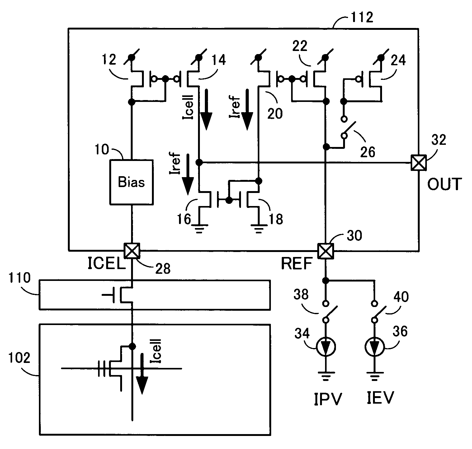
[0095] In a second embodiment, a flash EEPROM capable of setting a read reference with higher accuracy will be described. In the first embodiment, a method of setting a read reference using two current sources will be described. In general, a current source used in the first embodiment is composed of a transistor other than a double-gate structure transistor for use in a memory cell transistor, and a diode, a resistor, and the like. The reason is the following. If a double-gate structure transistor is used to construct a current source, a write operation needs to be performed with respect to a transistor contained in the current source in order to set a current flowing through the current source to be a predetermined value. However, a read reference which has been correctly set in advance is required to determine whether or not a write operation is correctly performed. Thus, there is a contradiction.

[0096] To avoid this situation, the write verification reference current IPV and th...

third embodiment

[0111] In a third embodiment, a flash EEPROM in which a reference cell and a memory cell array are disposed side by side will be described. In the second embodiment, a flash EEPROM comprising a reference cell composed of a transistor having the same structure as that of a memory cell is described. This flash EEPROM requires a circuit for supplying erase and write power sources to a reference cell. However, when a power source supply circuit specialized to a reference cell is provided, a circuit area is increased. Also, it is preferable that a read reference is provided on a block-by-block basis where each block is small, in order to further improve the accuracy of the read reference. According to the flash EEPROM of the third embodiment, such a problem can be solved.

[0112]FIG. 11 is a diagram illustrating a structure of a flash EEPROM according to the third embodiment of the present invention. The flash EEPROM 300 of FIG. 11 is different from the flash EEPROM 200 of the second embo...


PUM


Abstract

In a reference cell 202, first and second cells 50 and 52 having the same structure as that of a memory cell are provided. A memory cell current IREF1 of the first cell 50 is set to be a minimum value of a memory cell current after an erase operation. A memory cell current IREF2 of the second cell 52 is set to be a maximum value of a memory cell current after a write operation. The read circuit 206 compares a memory cell current Icell with a current (IREF1+IREF2)/2 and outputs a comparison result. A current source for use in erase verification and write verification may be used in place of the first and second cells 50 and 52.

Description

BACKGROUND OF THE INVENTION [0001] 1. Field of the Invention [0002] The present invention relates to a non-volatile semiconductor memory device. More particularly, the present invention relates to a method for reading the non-volatile semiconductor memory device, a method for setting a state of a reference cell, and a circuit for reading the non-volatile semiconductor memory device. [0003] 2. Description of the Background Art [0004] Non-volatile semiconductor memory devices are capable of holding data after turning OFF a power source, and therefore, are widely used in information systems, communication systems and the like. Flash EEPROM is a type of non-volatile semiconductor memory device, from which data can be erased for an entire chip or only on a block-by-block basis where the block has a predetermined size. The flash EEPROM has a small memory cell size and low manufacturing cost, so that its demand is rapidly increasing. [0005] A binary flash EEPROM controls the thresholds of ...

Claims


Application Information

Patent Timeline
Patent Type & Authority Applications(United States)
IPC IPC(8): G11C11/34
CPCG11C16/28
Inventor MORI, TOSHIKI
Owner CETUS TECH INC
Why Eureka
Try Eureka