Failure test method for split gate flash memory

a failure test and flash memory technology, applied in static storage, digital storage, instruments, etc., can solve the problems of reducing affecting the stability of the memory, and affecting the stability of the whole chip, so as to avoid the complicated analysis process and reduce the time for analyzing the memory

Active Publication Date: 2006-05-11
PROMOS TECH INC
View PDF5 Cites 48 Cited by
  • Summary
  • Abstract
  • Description
  • Claims
  • Application Information

AI Technical Summary

Benefits of technology

[0009] Accordingly, the present invention is directed to a failure test method for a split gate flash memory for easily and efficiently locating failure spots by using present electrical analyzing equipment.
[0017] The present invention uses the electrically analyzing method. After identifying the sector with the failed memory cell, all memory cells in the sector are programmed and read to generate a bit map. The bit map shows the location of failed bit-line. Then, all memory cells in the sector are erased and read to generate another bit map. The bit map shows the failed word-line location. By overlaying these bit maps, the location of the word line-bit line short circuit can be identified. Since all of these steps described above are performed in the same equipment, the time for analyzing the memory can be reduced. In addition, the equipment can be a general electricity analyzing equipment, but not necessarily the DC analyzing equipment, such as EMMI, LC, or OBIRCH. Thus, the complicated analyzing process can be avoided. Moreover, the present invention uses current-analyzing measurements and functional measurements to identify locations of defects, and is, therefore, different from the conventional location-analyzing method.

Problems solved by technology

If the over-erasing is so serious that the channel under the floating gate is turned on when power is not applied on the control gate, the data stored in the memory will be erroneously judged.
A disadvantage of this split gate flash memory cell is its vulnerability to defects, such as particles.
One single defect or particle may render the whole chip irreparable.
However, this method can only locate the defects, but cannot precisely identify the address of the word line-bit line short circuit, i.e. the main killer.
Moreover, the conventional method requires a complicated analyzing process, and cannot easily, efficiently locate the defects.

Method used


Image

  • Failure test method for split gate flash memory
  • Failure test method for split gate flash memory
  • Failure test method for split gate flash memory

Examples


Embodiment Construction

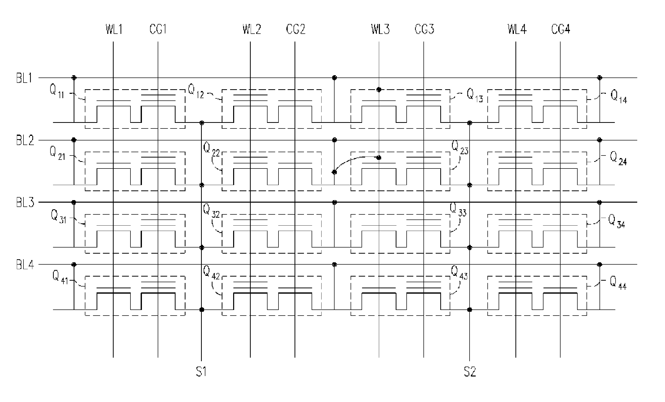
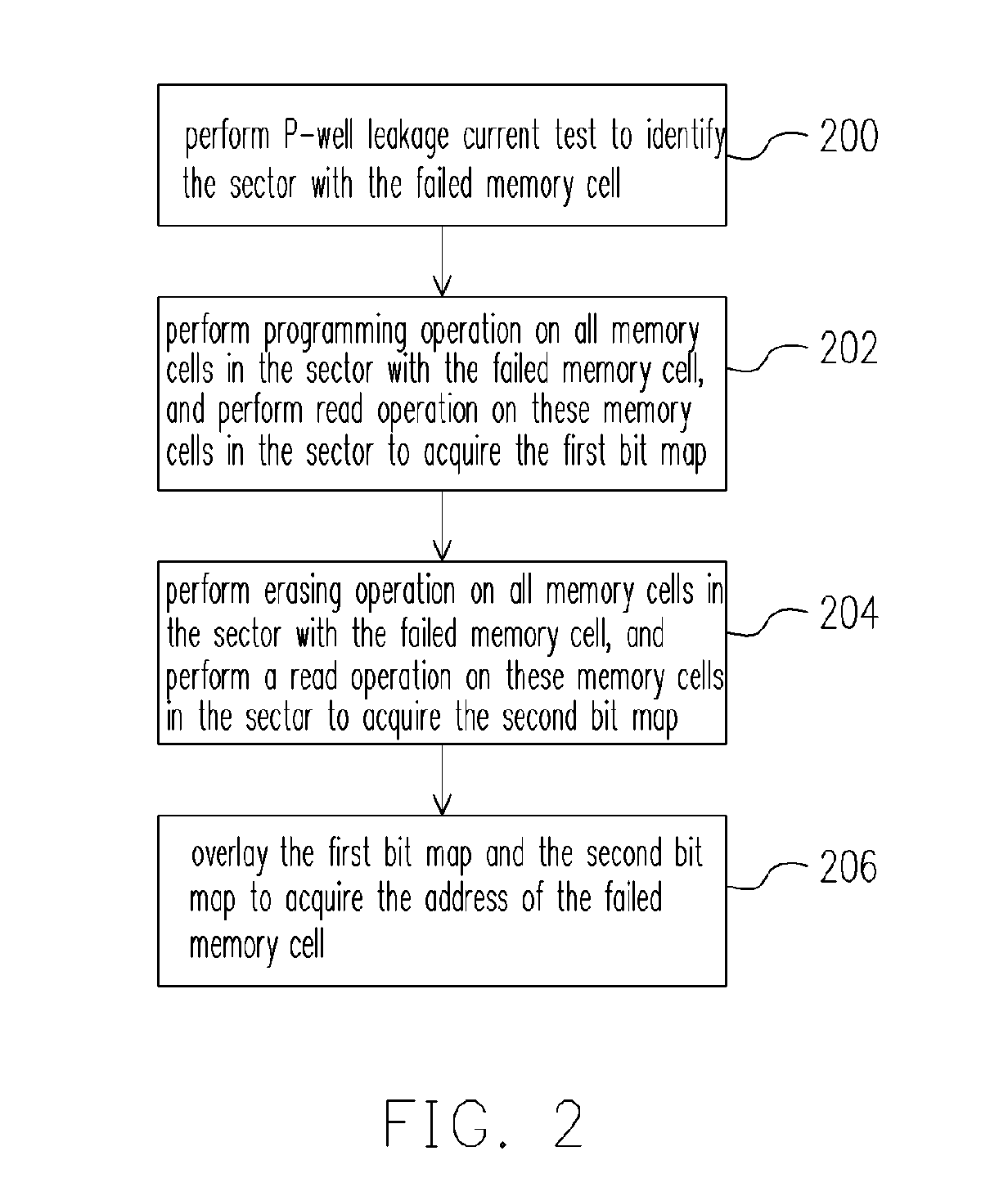
[0027]FIG. 2 is a flowchart showing a failure test method for a split gate flash memory according to an embodiment of the present invention. FIG. 3 is a schematic drawing showing an operation of a P-well leakage-current test for memory cells according to an embodiment of the present invention. In the following description, the failed memory cell is the memory cell where the word line-bit line short circuit occurs.

[0028] Referring to FIG. 2, the P-well leakage-current test is performed to identify the sector with the failed (defective) memory cell in the step 200. The P-well leakage-current test comprises, for example, applying 2V to the word line of the memory cell, and applying 8V to the substrate, i.e. the P-well, to measure current value of sectors as shown in FIG. 3. If a sector is a normal sector, the current measured is lower than 20 μA. When a sector contains a failed memory cell, a P-well leakage current is generated and the current measured is higher than 20 μA. For exampl...


PUM


Abstract

A failure test method of word line-bit line short circuit in a split gate flash memory is provided. A well leakage-current test is performed to identify a sector with a failed memory cell. After being programmed, memory cells in the sector undergo a first read operation to generate a first bit map of the sector. After being erased, these memory cells in the sector undergo a second read operation to generate a second bit map of the sector. The first bit map and the second bit map are overlaid to identify the actual address of the failed memory cell.

Description

BACKGROUND OF THE INVENTION [0001] 1. Field of the Invention [0002] The present invention relates to a test method for a semiconductor device, and more particularly to a failure test method for a split gate flash memory. [0003] 2. Description of the Related Art [0004] Flash memories can program, read and erase data for multiple times, and data stored therein can be maintained even if the power applied thereto is off. Therefore, flash memories have become the major non-volatile memory widely used in personal computers and electronic equipment. [0005] A typical flash memory comprises a floating gate and a control gate. The floating gate and the control gate are separated by a dielectric layer. The floating gate and the substrate are separated by a tunnel oxide layer. During data erasing in the flash memory, since the amount of electrons ejected from the floating gate is difficult to control, the floating gate would over-eject the electrons with positive charges, called over-erasing. I...

Claims


Application Information

Patent Timeline
Patent Type & Authority Applications(United States)
IPC IPC(8): G11C29/00
CPCG11C16/04G11C16/0425G11C29/02G11C29/025G11C29/44G11C29/50G11C29/50008G11C2029/5006
Inventor CHO, CHIH-HUNGTSAI, MING-SHIAHNHSU, SHIH-TSELIN, LIH-WEI
Owner PROMOS TECH INC
Why Eureka
Try Eureka