Method and apparatus for reviewing defect of subject to be inspected

a defect and defect technology, applied in the field of defect review methods and apparatuses, can solve the problems of heavy load on users, inability to efficiently select the view size of defect search in the defect review apparatus, and inability to efficiently carry out fine alignment. the effect of easy selection

Active Publication Date: 2006-05-18
HITACHI HIGH-TECH CORP
View PDF1 Cites 14 Cited by
  • Summary
  • Abstract
  • Description
  • Claims
  • Application Information

AI Technical Summary

Benefits of technology

[0015] Another object of the present invention is to provide a method and an apparatus for reviewing a defect, in which an error of defect coordinates output from an inspection apparatus is corrected so that the view size for defect search and a defect for fine alignment can be selected easily in the defect reviewing apparatus.
[0018] According to the present invention, the error of the defect coordinates output from the inspection apparatus can be corrected, and the view size for defect search and a defect for fine alignment can be selected easily in the defect reviewing apparatus.

Problems solved by technology

When there is an error in the defect coordinates output from the inspection apparatus as described above, the view size for defect search in the defect reviewing apparatus cannot be selected efficiently.
In addition, fine alignment cannot be carried out efficiently.
Accordingly, a heavy load is imposed on the user.
When correctable errors, that is, “nonrandom errors” are removed from the inspection coordinates, an uncorrectable error, that is, a “random error” is left in the inspection coordinates.

Method used


Image

  • Method and apparatus for reviewing defect of subject to be inspected
  • Method and apparatus for reviewing defect of subject to be inspected
  • Method and apparatus for reviewing defect of subject to be inspected

Examples


Embodiment Construction

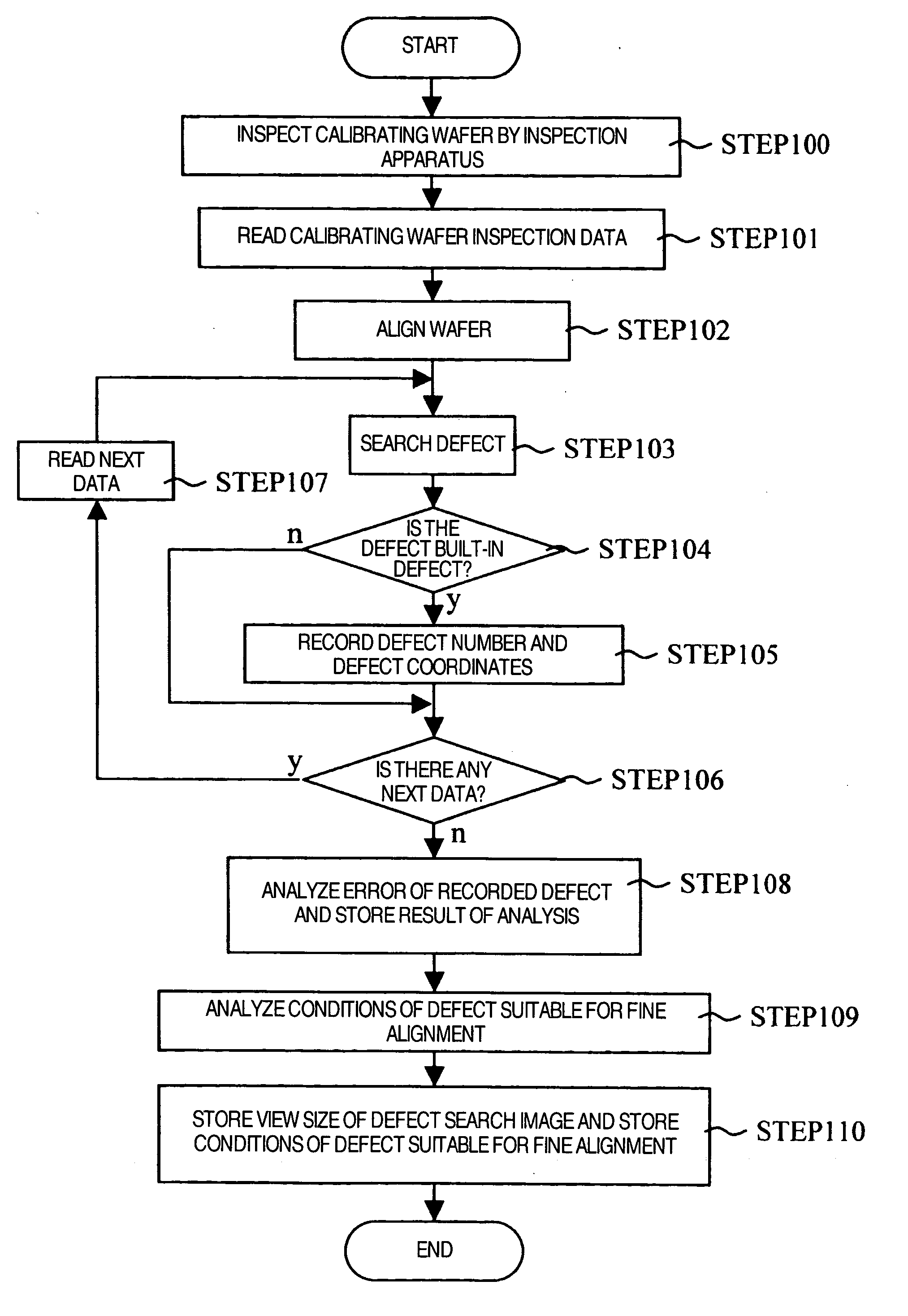
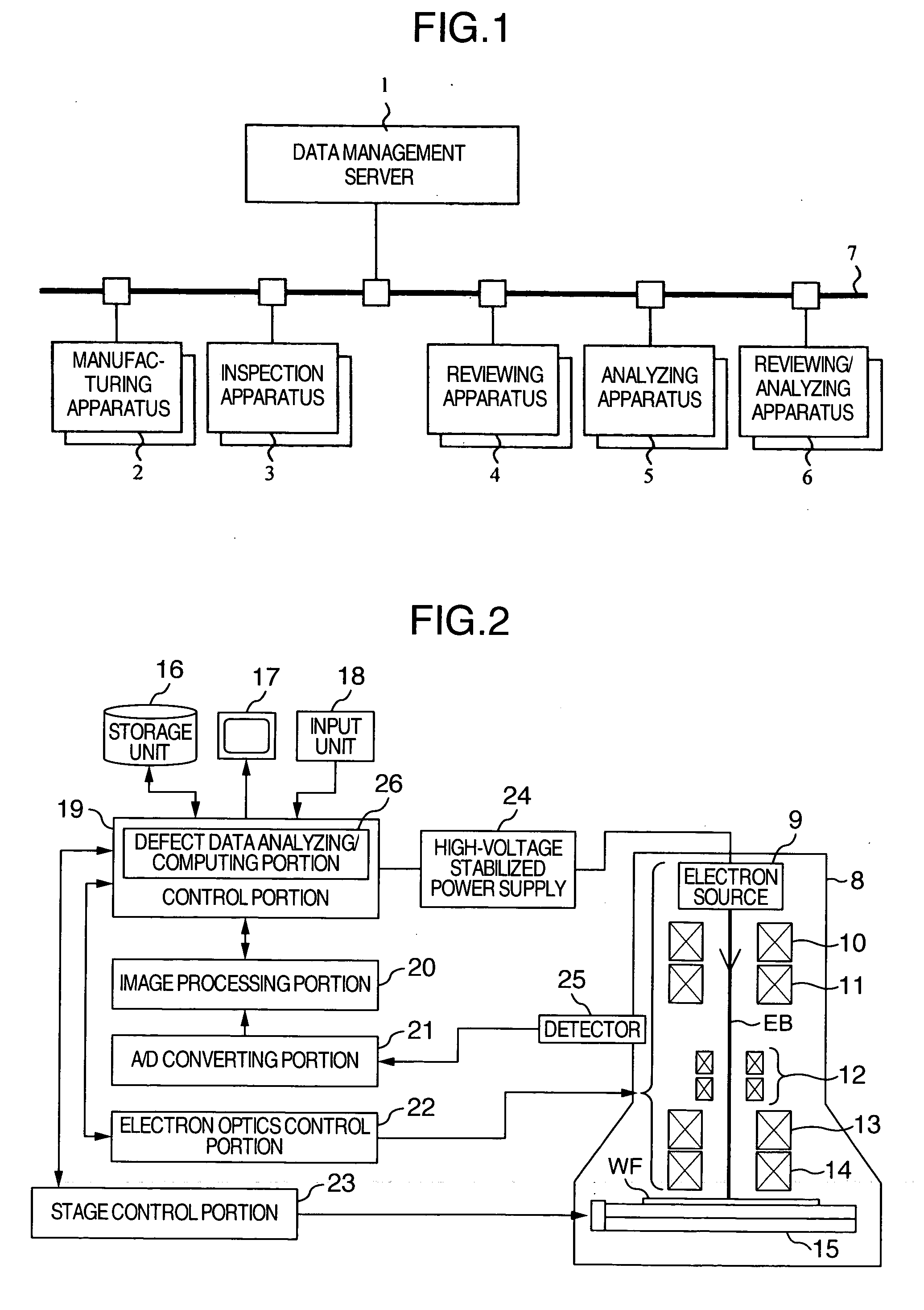
[0032] An embodiment of the present invention will be described below with reference to the drawings. First, with reference to FIG. 1, description will be made on a specific example of a connection configuration of pieces of apparatus provided in a semiconductor wafer manufacturing line. The semiconductor wafer manufacturing line includes a data management server 1, semiconductor wafer manufacturing apparatus 2, inspection apparatus 3, reviewing apparatus 4, analyzing apparatus 5 and reviewing / analyzing apparatus 6. These pieces of apparatus are connected to one another through a network 7.

[0033] The data management server 1 manages data obtained by the inspection apparatus 3, the reviewing apparatus 4, the analyzing apparatus 5 and the reviewing / analyzing apparatus 6.

[0034] The manufacturing apparatus 2 includes various kinds of units to be used for manufacturing a semiconductor wafer, such as an exposure unit, an etching unit, etc. The inspection apparatus 3 inspects a semicondu...


PUM


Abstract

Absolute coordinates designate position coordinates of a defect of a calibrating substrate, and inspection coordinates designate position coordinates of the defect of the calibrating substrate detected by an inspection apparatus. A deviation of the inspection coordinates with respect to the absolute coordinates is an error included in the inspection coordinates. When “nonrandom errors” are removed from the inspection coordinates, a “random error” is left in the inspection coordinates. The view size for defect search in a defect reviewing apparatus is set based on the random error. Further, a defect for fine alignment is selected based on the tendency of a detected value of the defect size of the calibrating substrate detected by the inspection apparatus.

Description

BACKGROUND OF THE INVENTION [0001] The present invention relates to a defect reviewing method and apparatus for zooming in on a defect of a thin-film device such as a semiconductor circuit substrate or a liquid crystal display substrate so as to review the defect. [0002] A thin-film device such as a semiconductor circuit device, a liquid crystal display or a magnetic head is manufactured through a large number of processes. For example, the number of processes may reach several hundreds. Accordingly, these thin-film devices are completed by processing with a large number of processing machines. When there is an abnormality in a processing machine or something unsatisfactory in manufacturing conditions, the fraction defective of final products will be increased to drop the yield. Therefore, processed substrates are inspected by use of an inspection apparatus. Due to time and labor constraints, it is impossible to inspect all the processed substrates in each manufacturing process. Usu...

Claims


Application Information

Patent Timeline
Patent Type & Authority Applications(United States)
IPC IPC(8): G06K9/00
CPCG01N21/9501
Inventor OBARA, KENJIAOKI, KAZUO
Owner HITACHI HIGH-TECH CORP
Why Eureka
Try Eureka