Optoelectronic transmitter integrated circuit and method of fabricating the same using selective growth process

a technology of optical transmitter and integrated circuit, which is applied in the direction of optics, optical elements, instruments, etc., can solve the problems of difficult to further improve the modulation efficiency and driving characteristic of the optical transmitter integrated circuit (ic), the conventional optical transmitter integrated circuit cannot be readily utilized for high-speed and long-distance optical communication, and the epitaxial structure cannot be independent and optimized. , to achieve the effect of simple fabrication of the oe transmitter integrated circuit, enhancing the coupling and modul

Inactive Publication Date: 2006-05-25
ELECTRONICS & TELECOMM RES INST
View PDF4 Cites 2 Cited by
  • Summary
  • Abstract
  • Description
  • Claims
  • Application Information

AI Technical Summary

Benefits of technology

[0008] The present invention is directed to an optoelectronic (OE) transmitter integrated circuit (IC) and method of fabricating the same, in which a multi-quantum well (MQW) absorption layer of an electroabsorption (EA) modulator is formed to a thicker thickness using a selective MOCVD growth process so as to enhance the coupling and modulation efficiency of the EA modulator. Also, the EA modulator is integrated as a single chip on a semi-insulating substrate along with a driving circuit fabricated using the DHBT, which amplifies small electric signals to the high gained large electrical signal, so that the fabrication of the OE transmitter integrated circuit is simple.

Problems solved by technology

For this reason, the conventional optical transmitter integrated circuit cannot be readily utilized for high-speed and long-distance optical communications.
However, since a conventional pin type EA modulator has the same epitaxial crystal structure as a DHBT consisting of p+-base, i-collector and n+-sub collector, it cannot have an independent epitaxial structure and optimize its characteristics.
Thus, it is difficult to further improve the modulation efficiency and driving characteristic of the optical transmitter integrated circuit (IC).

Method used


Image

  • Optoelectronic transmitter integrated circuit and method of fabricating the same using selective growth process
  • Optoelectronic transmitter integrated circuit and method of fabricating the same using selective growth process
  • Optoelectronic transmitter integrated circuit and method of fabricating the same using selective growth process

Examples


Embodiment Construction

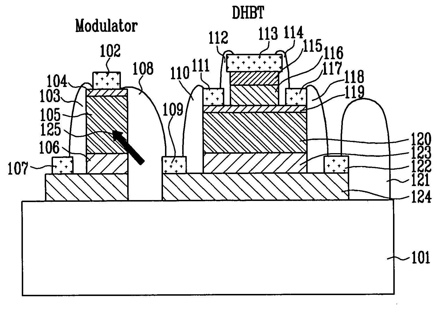
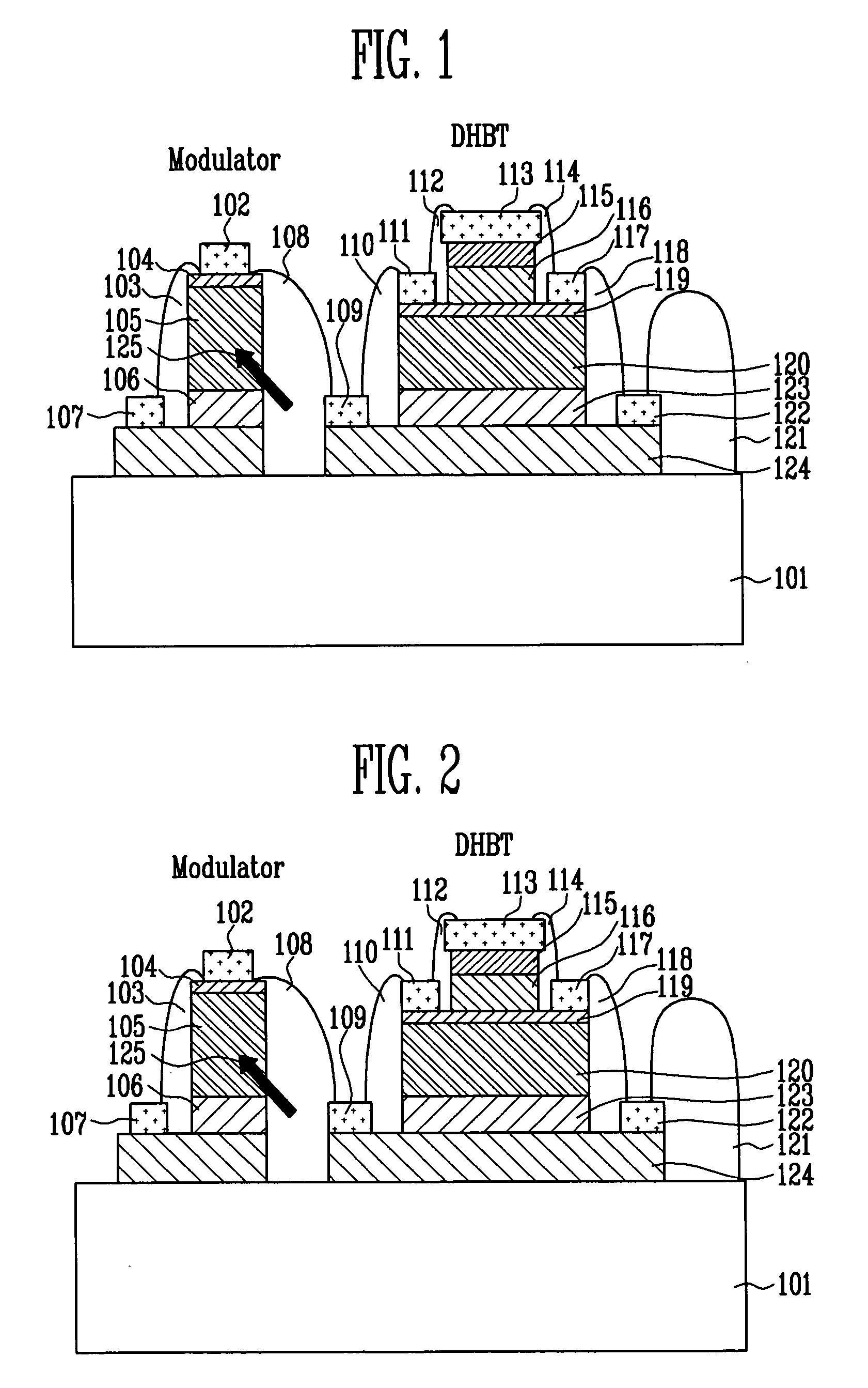
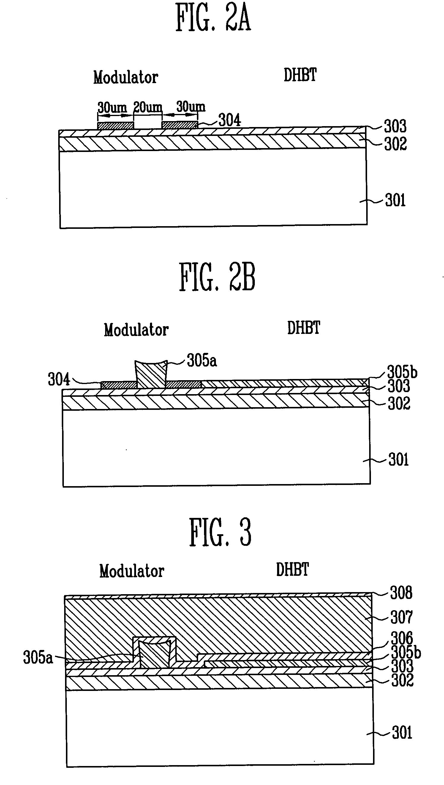
[0023] The present invention will now be described more fully hereinafter with reference to the accompanying drawings, in which exemplary embodiments of the invention are shown. In the embodiments of the present invention, an electroabsorption (EA) modulator formed of n-InP / multi-quantum well (MQW) i-InGaAs—InP / p+InGaAs and a double heretojunction bipolar transistor (DHBT) formed of n-InP / MQW i-InGaAs—InP / p+InGaAs / n-InP, which are formed on a semi-insulating InP substrate, are exemplarily described. This invention may, however, be embodied in different forms and should not be construed as limited to the embodiments set forth herein. Rather, these embodiments are provided so that this disclosure is thorough and complete and fully conveys the scope of the invention to those skilled in the art. In the drawings, the thicknesses of layers may be exaggerated for clarity, and the same reference numerals are used to denote the same elements throughout the drawings.

[0024]FIG. 1 is a cross s...


PUM


Abstract

Provided are an optoelectronic (OE) transmitter integrated circuit (IC) and method of fabricating the same using a selective growth process. In the OE transmitter IC, a driving circuit, which includes a double heterojunction bipolar transistor (DHBT) and amplifies received electric signals to drive an electroabsorption (EA) modulator, and the EA modulator with a multi-quantum well (MQW) absorption layer are integrated as a single chip on a semi-insulating substrate. The MQW absorption layer of the EA modulator and an MQW insertion layer of the DHBT are formed to different thicknesses from each other using a selective MOCVD growth process.

Description

CROSS-REFERENCE TO RELATED APPLICATION [0001] This application claims priority to and the benefit of Korean Patent Application No. 2004-95949, filed Nov. 22, 2004, the disclosure Of which is incorporated herein by reference in its entirety. BACKGROUND [0002] 1. Field of the Invention [0003] The present invention relates to an optoelectronic transmitter integrated circuit and method of fabricating the same and, more specifically, to an optoelectronic transmitter integrated circuit having an integrated single chip structure in which an absorption layer of an electroabsorption (EA) modulator and a quantum well (QW) layer of a double heretojunction bipolar transistor (DHBT) have different thicknesses, and method of fabricating the same using a selective MOCVD (Metal Organic Chemical Vapor Deposition) growth method. [0004] 2. Discussion of Related Art [0005] A conventional long-wavelength optical transmitter integrated circuit in which a semiconductor laser and a DHBT are integrated is w...

Claims


Application Information

Patent Timeline
Patent Type & Authority Applications(United States)
IPC IPC(8): H01L29/06H01L31/0328
CPCB82Y20/00G02F1/017H01L31/18G02B26/00H01S5/34
Inventor NAM, EUN SOOKIM, YONG WONHONG, SEON EUIOH, MYUNG SOOKKIM, BO WOO
Owner ELECTRONICS & TELECOMM RES INST
Why Eureka
Try Eureka