Light emitting diode chip with large heat dispensing and illuminating area

a technology of light-emitting diodes and heat-dispensing diodes, which is applied in the direction of basic electric elements, electrical equipment, semiconductor devices, etc., can solve the problems of poor heat dissipation ability of conventional light-emitting diodes, inherent drawbacks of high temperature, etc., and achieve the effect of increasing the efficiency of heat dissipation, increasing the electrical conductivity, and increasing the area of electricity conducting area

Inactive Publication Date: 2006-06-01
YANG CHIU CHUNG
View PDF3 Cites 15 Cited by
  • Summary
  • Abstract
  • Description
  • Claims
  • Application Information

AI Technical Summary

Benefits of technology

[0007] The present invention provides a light emitting diode chip wherein the etching process does not reduce the illuminating area and a large area of electricity conducting area is applied to each of the P pole and the N pole so that the areas of illumination and reflection are increased and the efficiency for dispensing heat is increased. The light emitting diode chip needs no encapsulation and includes functions as those flip chips and SMD.

Problems solved by technology

As shown in FIG. 3, the conventional chip has poor ability for dispensing heat, because the length “L” for the paths is tool long and the area “S” for dispensing heat is small so that the conventional light emitting diode chip has an inherent drawback of high temperature.

Method used


Image

  • Light emitting diode chip with large heat dispensing and illuminating area
  • Light emitting diode chip with large heat dispensing and illuminating area
  • Light emitting diode chip with large heat dispensing and illuminating area

Examples


Embodiment Construction

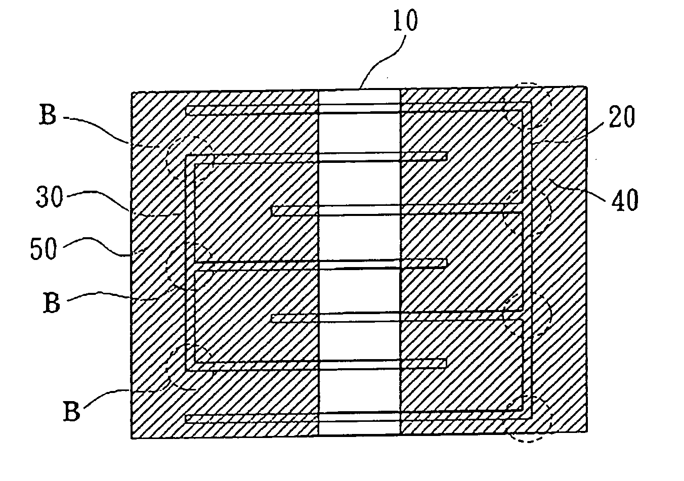
[0016] Referring to FIG. 5, the light emitting diode chip 10 has a P pole 20 and an N pole 30 on one side thereof and this side of the chip 10 is treated by an etching process. Two large areas of electricity conductive materials 40 and 50 are applied to the P pole 20 and an N pole 30 respectively. By the large areas of the of electricity conductive materials 40 and 50, the chip 10 has a large area for dispensing heat and for reflecting light with encapsulation. The areas of the P pole 20 and an N pole 30 are also enlarged. The chip 10 of the present invention includes all the functions of SMD and flip chips so that the expense for encapsulation can be reduced.

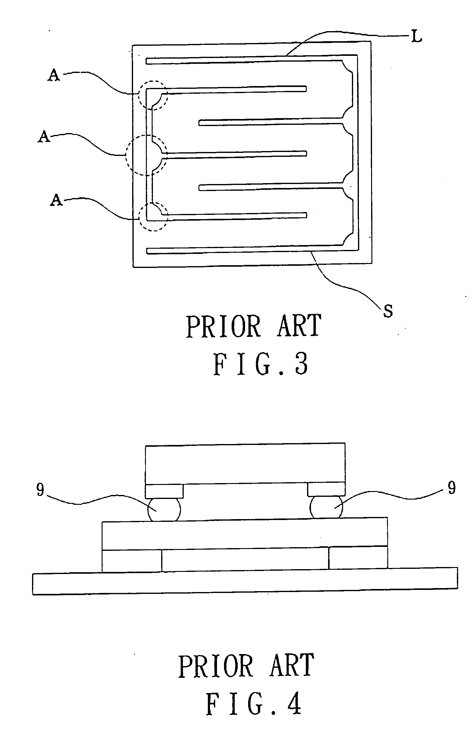
[0017] As shown in FIG. 6, the difference between the chip 10 of the present invention an the conventional chip can be seen when compared with the chip shown FIG. 3, wherein the “A” in FIG. 3 is the position for wiring so that the etching area is large. The chip of the present invention needs no wiring so that the area for etc...


PUM


Abstract

A light emitting diode chip has a large area of electricity conducting material applied to each of the P pole and the N pole and the etching process does not reduce the illuminating area so that the areas of illumination and reflection are increased and the efficiency for dispensing heat is increased. The light emitting diode chip needs no encapsulation and includes functions as those flip chips and SMD.

Description

FIELD OF THE INVENTION [0001] The present invention relates to a light emitting diode chip with large area of heat dispensing and illuminating area. BACKGROUND OF THE INVENTION [0002] A conventional light emitting diode chip is shown in FIG. 1 and generally includes an N pole 1 and a P pole 2, and one of the two poles 1, 2 has an etching 3 which reduces the illuminating layer 4 of the chip so that the illumination is reduced which cannot meet requirement in the market. Besides, as shown in FIGS. 2 and 3, the chip 5 has a compact size and the area “A” for wiring 8 to the N pole 6 and P pole 7 is much larger than conventional light emitting diode chips so that the illuminating area is very limited. Generally, the area for wiring is around 100μ. [0003]FIG. 2 shows a welding technique named SMD to the light emitting diode chip wherein the chip 5 has to reserve the wiring position so that the chip 5 can be connected to the base board by the wires and the base board is then electrically c...

Claims


Application Information

Patent Timeline
Patent Type & Authority Applications(United States)
IPC IPC(8): H01L33/00H01L33/40H01L33/62
CPCH01L33/20H01L33/38H01L33/405H01L33/486H01L33/62H01L2224/16H01L2224/48091H01L2224/49107H01L2924/01079H01L2924/00014H01L2924/12041H01L2224/05573H01L2224/05568H01L2224/05111H01L2224/05124H01L2224/05139H01L2224/05144H01L2224/05147H01L2224/05611H01L2224/05624H01L2224/05639H01L2224/05644H01L2224/05647H01L24/05
Inventor YANG, CHIU-CHUNG
Owner YANG CHIU CHUNG
Why Eureka
Try Eureka