

Display device
Inactive Publication Date: 2006-06-01
TOSHIBA MATSUSHITA DISPLAY TECH
View PDF11 Cites 49 Cited by
- Summary
- Abstract
- Description
- Claims
- Application Information
AI Technical Summary
Benefits of technology
[0008] The object of the invention is to provide a display device, which can suppress degradation of self-luminous display elements and can realize a high display quality and a long lifetime.
[0010] The present invention can provide a display device, which can suppress degradation of self-luminous display elements and can realize a high display quality and a long lifetime.
Problems solved by technology
In the case where the driving circuit board is fixed in close contact with the display panel, as described above, there is a fear that the temperature of the display panel rises due to radiation heat from the driving circuit and the lifetime of the self-luminous elements becomes shorter.
Method used
View moreImage
Smart ImageViewing Examples

Examples
example
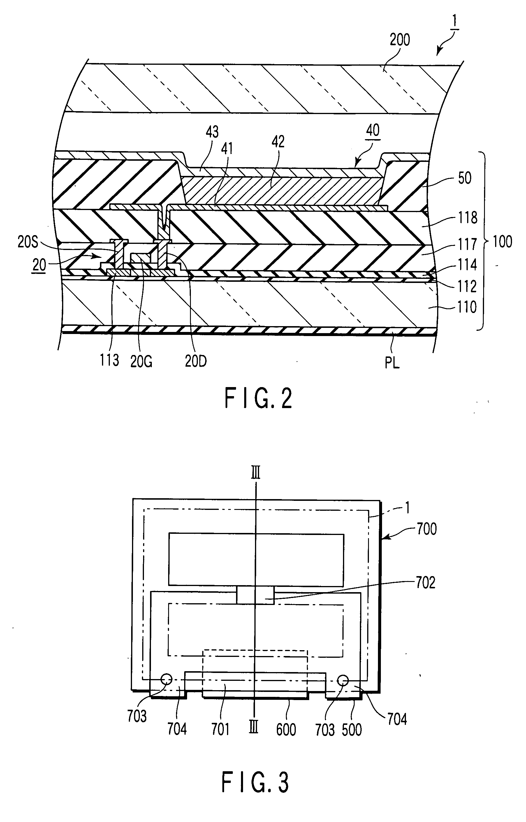
[0043] In an organic EL display device with the above-described structure, a gap G of 0.1 mm was provided between the display panel 1 and the driving circuit board 500 having the single-side mounting structure. As regards this structure, the temperature of the display panel 1 before turn-on of power was compared with the temperature of the display panel 1 in the state in which a variation in temperature was stabilized after turn-on of power. The temperature of the display panel 1 rose by 5° C.
Login to View More PUM
 Abstract
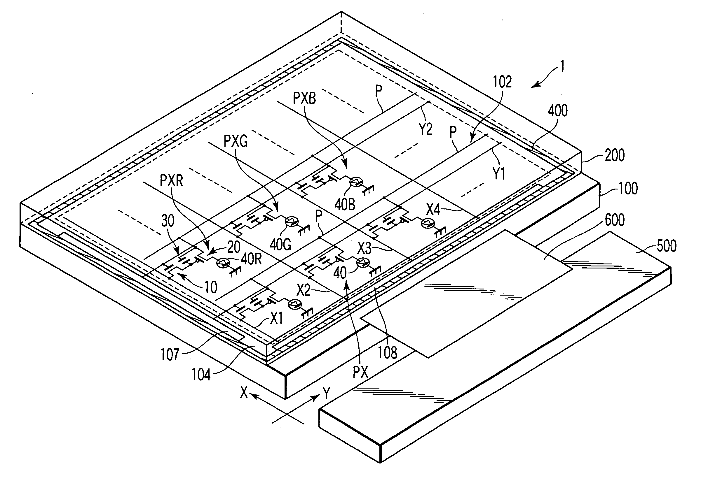
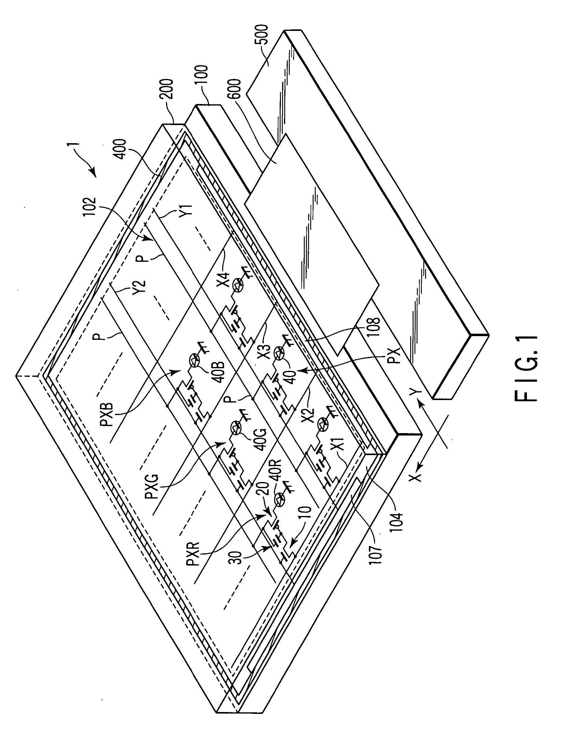
A display device includes a display panel having a self-luminous display element on a substrate and having one major surface as a display surface, a driving circuit board that is connected to the display panel via a flexible board, is disposed on a non-display-surface-side of the display panel, and supplies a driving signal to the display panel, and a heat resistance layer that is disposed between the display panel and the driving circuit board.
Description
CROSS-REFERENCE TO RELATED APPLICATIONS [0001] This application is based upon and claims the benefit of priority from prior Japanese Patent Application No. 2004-342560, filed Nov. 26, 2004, the entire contents of which are incorporated herein by reference. BACKGROUND OF THE INVENTION [0002] 1. Field of the Invention [0003] The present invention relates generally to a display device, and more particularly to a display device that is composed of self-luminous display elements. [0004] 2. Description of the Related Art [0005] In recent years, organic electroluminescence (EL) display devices have attracted attention as flat-panel display devices. The organic EL display device comprises self-luminous elements. Thus, it has such features as a wide viewing angle, small thickness without a need for backlight, low power consumption, and a high responsivity speed. [0006] For these features, attention has been paid to the organic EL display device as a promising candidate for the next-generatio...
Claims
Login to View More Application Information
Patent Timeline
 IPC IPC(8): H05B33/06H05B33/08H05B44/00
CPCG09G3/3225G09G3/3233G09G2300/0426G09G2300/0842H01L27/3244H01L27/3276H01L51/529H10K59/12H10K59/131H10K59/8794H10K50/87
InventorNAKAMURA, NORIO
OwnerTOSHIBA MATSUSHITA DISPLAY TECH