This helps you quickly interpret patents by identifying the three key elements:
Problems solved by technology
Method used
Benefits of technology
Benefits of technology
[0013]In the above configuration, since the via wires out at least one of the first line and the second line to the same side of the insulating layer as the other one of the first and the second lines, the first and second lines can share wiring layers in which the respective lines are to be formed. As a result, the number of layers in the coupler is reduced and this reduction of layers allows a thinner coupler, and such a thinner coupler has a reduced size. Since there is no need to reduce the lengths of the first and second lines in the coupler according to the invention, a thinner coupler with a reduced size can be obtained without decreasing the coupling in the coupler.
[0022]It is preferable that the above coupler further has a via connected to the main line or the secondary line and extending through the insulating layer, the via wiring out at least one the first line and the second line to the same side of the insulating layer as the other one of the first and second lines. In the above, the coupler of the invention may have: a first layer including at least the main line; a second layer including at least the secondary line; and a third layer including at least part of the first connecting wiring and / or the second connecting wiring. By wiring out, using the via, at least one of the first line and the second line to the same side of the insulating layer as the other one of the first and second lines, the first line and the second line can share wiring layers in which the respective lines are to be formed, and thus, the number of layers in the coupler can be reduced, which contributes to producing a thinner coupler.
Problems solved by technology
However, there are limits to producing thinner and smaller couplers using the conventional coupler configuration where the main line and the secondary line are each wired out to the opposite sides of the insulating layer through the vias.
On the other hand, if the size of the coupler is simply reduced to obtain a thinner and smaller coupler, the lines, e.g., coils, constituting the coupler are inevitably shortened, which would decrease the coupling in the coupler.
Furthermore, if the number of windings of the coil is increased to increase the coupling in the coupler, unnecessary coupling would increase as well between portions of the same line existing in the same layer, resulting in a problem of degraded directivity or isolation properties.
Method used
Image
Click on the blue label to locate the original text in one second.
Reading with bidirectional positioning of images and text.
Examples
embodiment 1
[0066]Next, one example of the respective patterns of the wiring layers M1, M2 and M3 in a coupler of Embodiment 1 will be described in detail. In the below embodiment, coils are used for the main line and the secondary line which constitute the lines L1 and L2 respectively.
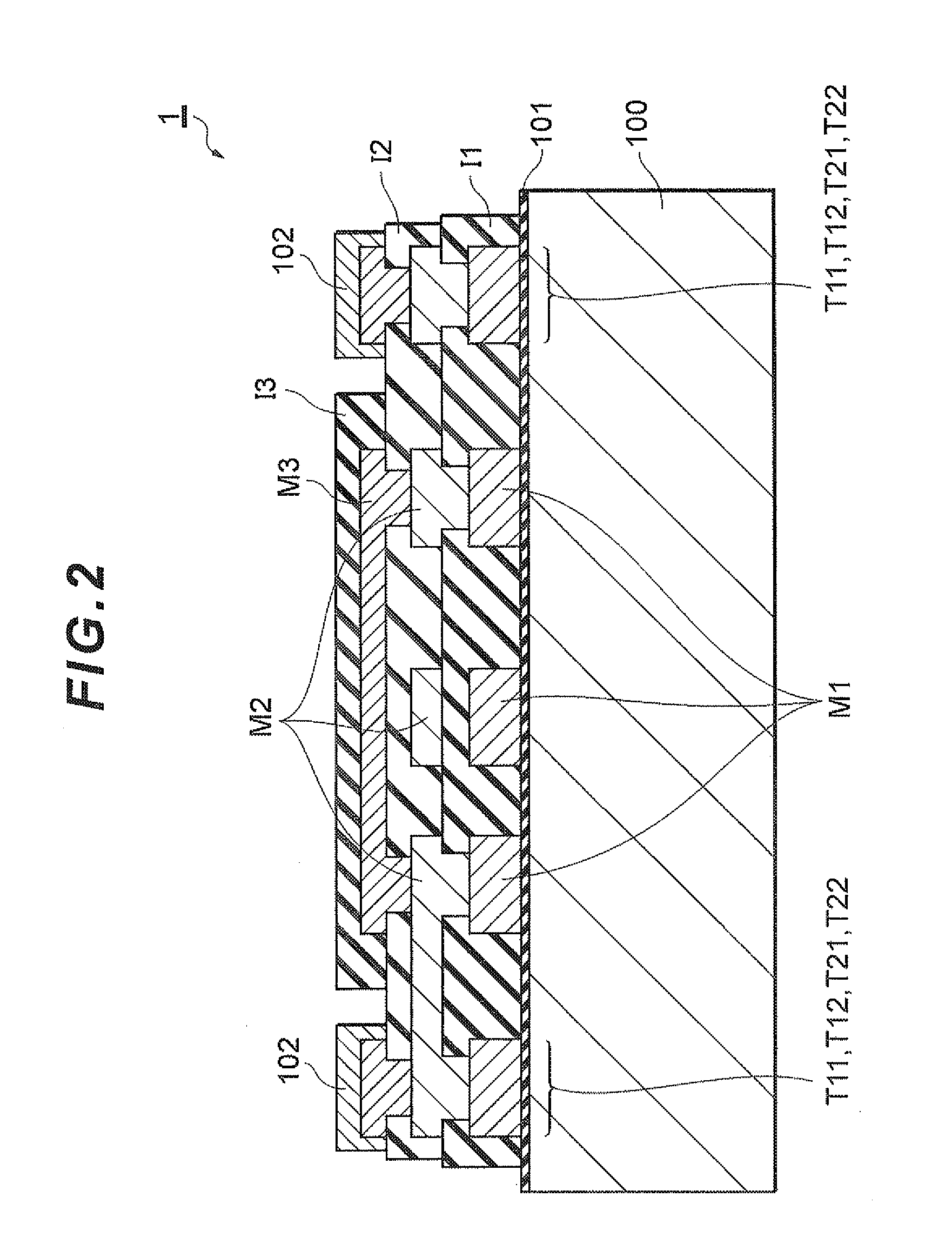
[0067]FIGS. 3-8 are horizontal sectional views schematically illustrating the respective layers M1-M3 and I1-I3 of the coupler 1. As illustrated in FIGS. 3-8, the input terminal T11, the output terminal T12, the coupling terminal T21, and the isolation terminal T22 are formed in all the wiring layers M1-M3, and the portions of the terminals T11, T12, T21 and T22 formed in one layer are electrically connected to the corresponding portions in a different layer. The following is a detailed explanation of the configuration of each layer.
[0068]Referring to FIG. 3, in the wiring layer M1 formed on the insulating substrate 100 (via the insulating film 101), the coiled first line L1 is formed. In the wiring layer M1, the...
embodiment 1a
[0085]Next, the respective patterns of the wiring layers M1, M2 and M3 in a coupler according to Embodiment 1A will be described in detail. FIGS. 11-16 are horizontal sectional views schematically illustrating the respective layers M1-M3 and I1-I3 of a coupler 1A. As illustrated in FIGS. 11-16, the input terminal T11, the output terminal T12, the coupling terminal T21, and the isolation terminal T22 are formed in all the wiring layers M1-M3, and the portions of the terminals T11, T12, T21 and T22 formed in one layer are electrically connected to the corresponding portions in a different layer. The following is a detailed explanation of the configuration of each layer.
[0086]Referring to FIG. 11, in the wiring layer M1 formed on the insulating substrate 100 (via the insulating film 101), the coiled first line L1 is formed. In the wiring layer M1, the outer end of the coiled first line L1 is connected to the output terminal T12, and the inner end of the first line L1 is connected to th...
embodiment 1b
[0097]Next, the configuration of a coupler according to Embodiment 1B will be described. FIGS. 18-22 are horizontal sectional views schematically illustrating the respective layers M1-M3 and I1-I2 of a coupler 1B. The pattern of the passivation layer I3 of Embodiment 1B is the same as that of Embodiment 1A. Also, as with Embodiment 1, the terminals T11,T12,T21 and T22 are formed in all the wiring layers M1-M3. Referring to FIG. 18, in the wiring layer M1 formed on the insulating substrate 100 (via the insulating film 101), the coiled first line L1 is formed. In Embodiment 1B, the first line L1 formed in the wiring layer M1 has a different number of windings from that of Embodiment 1A, and the position of the inner end also differs from Embodiment 1A. Accordingly, the via P11 of Embodiment 1A, which is connected to the inner end of the first line L1, is arranged in an area close to the isolation terminal T22 (see FIG. 11); whereas, the via P11 of Embodiment 1B, which is connected to ...
PUM
Abstract
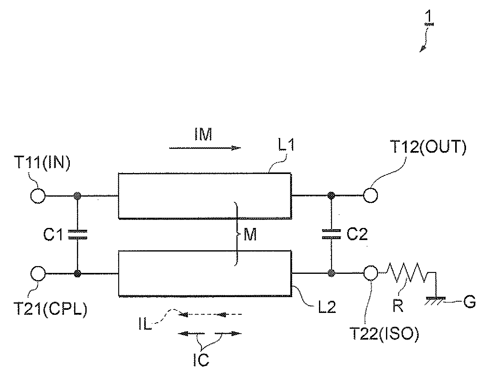
The invention provides couplers that are thinner and smaller in size and still satisfy the required various properties of the couplers.According to an embodiment of the invention, a coupler has a first line L1 that includes a coiled main line L11 and is constituted by separate portions arranged in different layers; a second line L2 that includes a coiled secondary line L21 arranged to be opposed to the main line L11 via an insulating layer, the second line being constituted by separate portions arranged in different layers; a plurality of vias P11, P12, P21 and P22 that connect the separate portions of the first line arranged in the different layers to each other and connect the separate portions of the second line arranged in the different layers to each other; and a plurality of terminals T11, T12, T21 and T22 each connected to an end of the first and second lines L1 and L2. The vias include an extension via P11 connected to the main line or the secondary line and extending through the insulating layer, and the extension via P11 wires out at least one of the first line L1 and the second line L2 to the same side of the insulating layer as the other one of the first line L1 and the second line L2.
Description
CROSS-REFERENCES TO RELATED APPLICATIONS[0001]The present application relates to and claims priority from Japanese Patent Application Nos. 2009-272227 and 2009-272231, both filed on Nov. 30, 2009, the entire disclosure of which is incorporated herein by reference.BACKGROUND[0002]1. Field of the Invention[0003]The present invention relates to a directional coupler (hereinafter simply referred to as a “coupler”) that picks up part of an output signal, and particularly relates to a coupler formed by a thin-film formation process which is advantageous for achieving thinner products with smaller sizes.[0004]2. Description of Related Art[0005]Radio communication devices are constituted by various kinds of high-frequency components such as antennas, filters, RF switches, power amplifiers, couplers, baluns, etc. In general, a coupler is used for the purpose of picking up part of an output of a power amplifier and feeding it back to an input to the power amplifier so as to maintain and contr...
Claims
Application Information
Patent Timeline
Application Date:The date an application was filed.
Publication Date:The date a patent or application was officially published.
First Publication Date:The earliest publication date of a patent with the same application number.
Issue Date:Publication date of the patent grant document.
PCT Entry Date:The Entry date of PCT National Phase.
Estimated Expiry Date:The statutory expiry date of a patent right according to the Patent Law, and it is the longest term of protection that the patent right can achieve without the termination of the patent right due to other reasons(Term extension factor has been taken into account ).
Invalid Date:Actual expiry date is based on effective date or publication date of legal transaction data of invalid patent.

