High speed DRAM cache architecture

a cache architecture and high-speed technology, applied in the field of cache memories, can solve the problems of high cost of cache memory and general cost ris

Inactive Publication Date: 2006-06-01
INTEL CORP
View PDF7 Cites 9 Cited by
  • Summary
  • Abstract
  • Description
  • Claims
  • Application Information

AI Technical Summary

Problems solved by technology

However, cache memory is often expensive, and generally costs rise as cache speed and size increase.

Method used


Image

  • High speed DRAM cache architecture
  • High speed DRAM cache architecture
  • High speed DRAM cache architecture

Examples


Embodiment Construction

[0017] The following description provides a high speed cache architecture. In the following description, numerous specific details are set forth in order to provide a more thorough understanding of the present invention. It will be appreciated, however, by one skilled in the art that the invention may be practiced without such specific details. In other instances, control structures and gate level circuits have not been shown in detail in order not to obscure the invention. Those of ordinary skill in the art, with the included descriptions, will be able to implement appropriate logic circuits without undue experimentation.

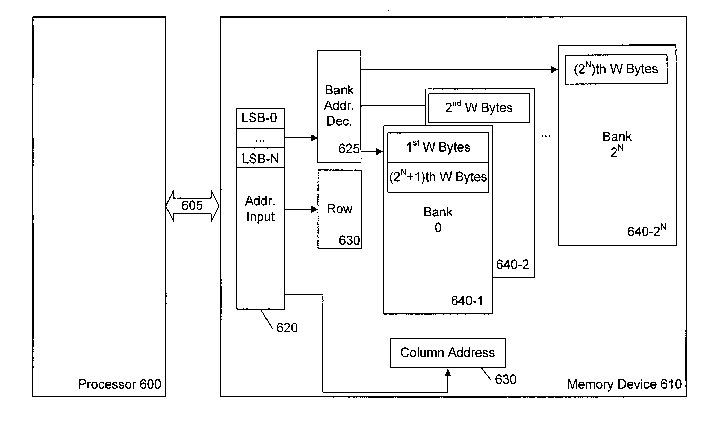
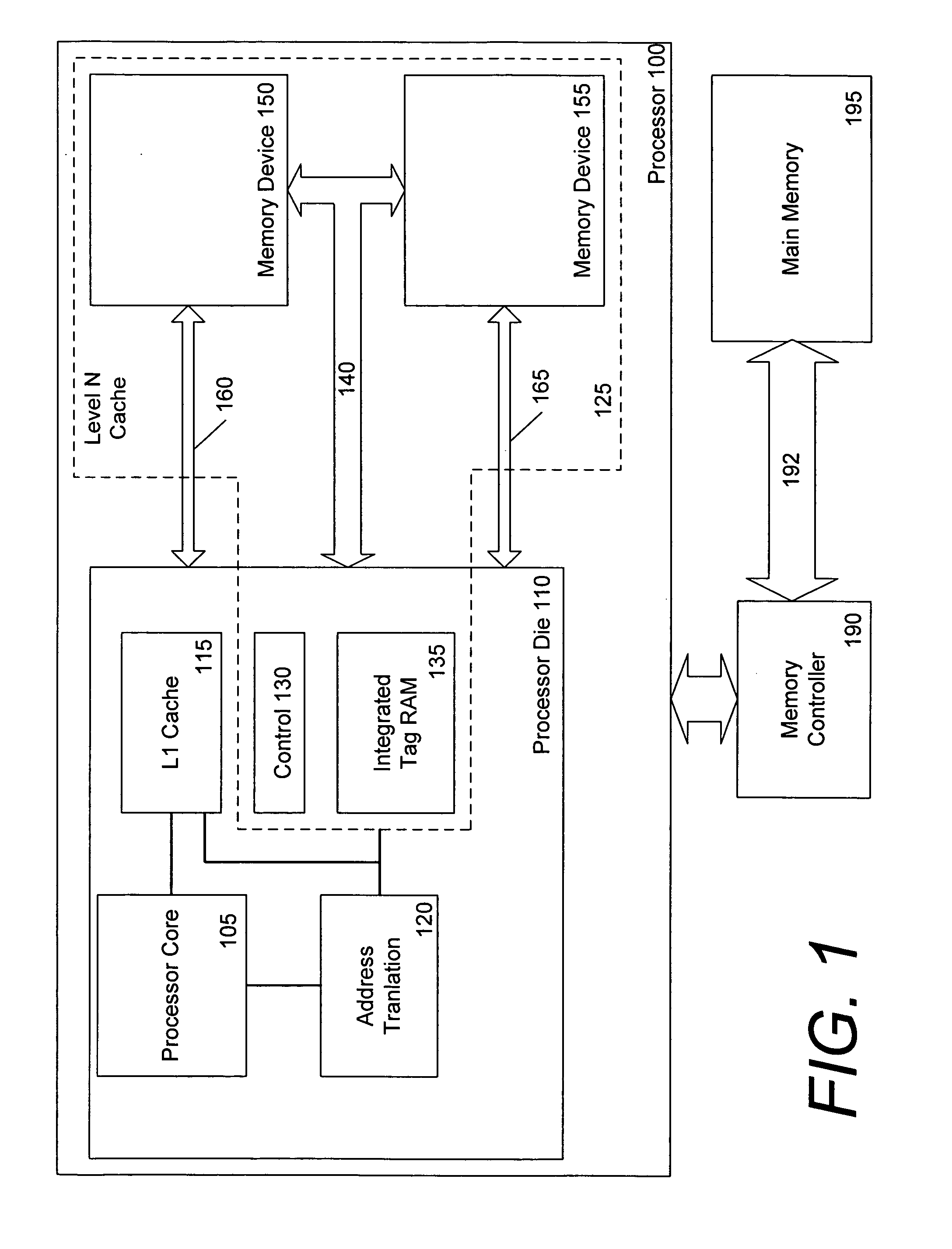
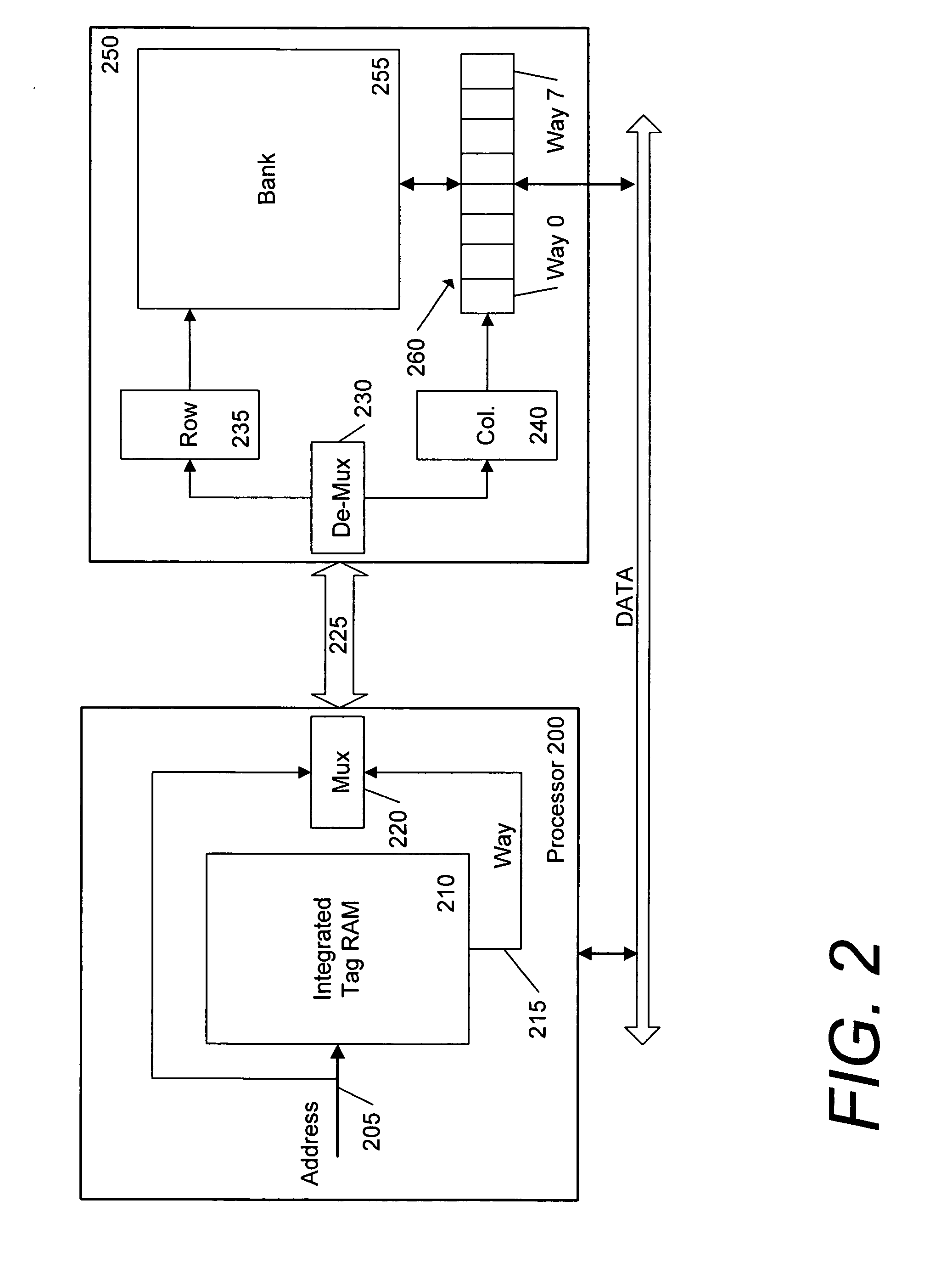
[0018] Various embodiments disclosed may allow a high density memory such as a DRAM memory to be efficiently used as cache memory. Some embodiments provide particular cache way and / or bank mapping techniques that may be advantageous in particular situations. Some embodiments effectively pipeline tag lookups with memory access cycles to reduce memory access latency...


PUM


Abstract

A high speed DRAM cache architecture. One disclosed embodiment includes a multiplexed bus interface to interface with a multiplexed bus. A cache control circuit drives a row address portion of an address on the multiplexed bus interface and a command to open a memory page containing data for a plurality of ways. The cache control circuit subsequently drives a column address including at least a way indicator to the multiplexed bus interface.

Description

CROSS-REFERENCE TO RELATED APPLICATIONS [0001] This application is a continuation of U.S. patent application Ser. No. 10 / 210,908 entitled “High Speed DRAM Cache Architecture”, filed Aug. 2, 2002 and assigned to the assignee of the present application, which is related to U.S. patent application Ser. No. 10 / 211,680, now U.S. Pat. No. 6,954,822, entitled “Techniques to Map Cache Data to Memory Arrays”, filed Aug. 2, 2002 and assigned to the assignee of the present application.BACKGROUND [0002] 1. Field [0003] The present disclosure pertains to the field of cache memories. More particularly, the present disclosure pertains to a new cache architecture using a dynamic random access memory (DRAM) or the like and methods of mapping cache entries into the memory. [0004] 2. Description of Related Art [0005] Cache memories generally improve memory access speeds in computer or other electronic systems, thereby typically improving overall system performance. Increasing either or both of cache s...

Claims


Application Information

Patent Timeline
Patent Type & Authority Applications(United States)
IPC IPC(8): G06F12/08G06F12/00
CPCG06F12/0864G06F12/0882G06F12/0893
Inventor BAINS, KULJIT S.HUM, HERBERTHALBERT, JOHN
Owner INTEL CORP
Why Eureka
Try Eureka