Phase changeable memory cells and methods of forming the same

a memory cell and phase change technology, applied in the field of semiconductor devices, can solve problems such as the instability of the and achieve the effect of stable interface between the phase change material layer and the silicon layer of the conventional memory cell

Inactive Publication Date: 2006-06-08
SAMSUNG ELECTRONICS CO LTD
View PDF12 Cites 252 Cited by
  • Summary
  • Abstract
  • Description
  • Claims
  • Application Information

AI Technical Summary

Problems solved by technology

Consequently, the phase change material layer of the phase changeable memory cell described in the Wu patent is in direct contact with silicon layers, which in

Method used


Image

  • Phase changeable memory cells and methods of forming the same
  • Phase changeable memory cells and methods of forming the same
  • Phase changeable memory cells and methods of forming the same

Examples


examples

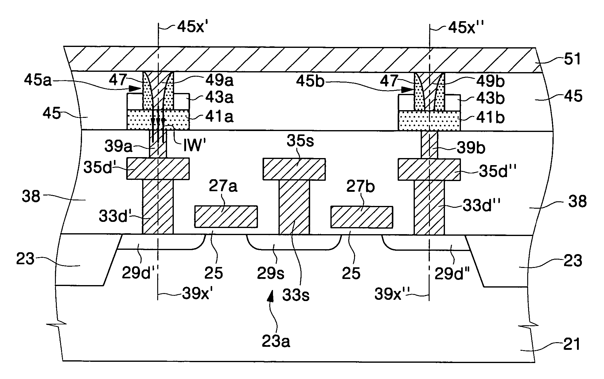
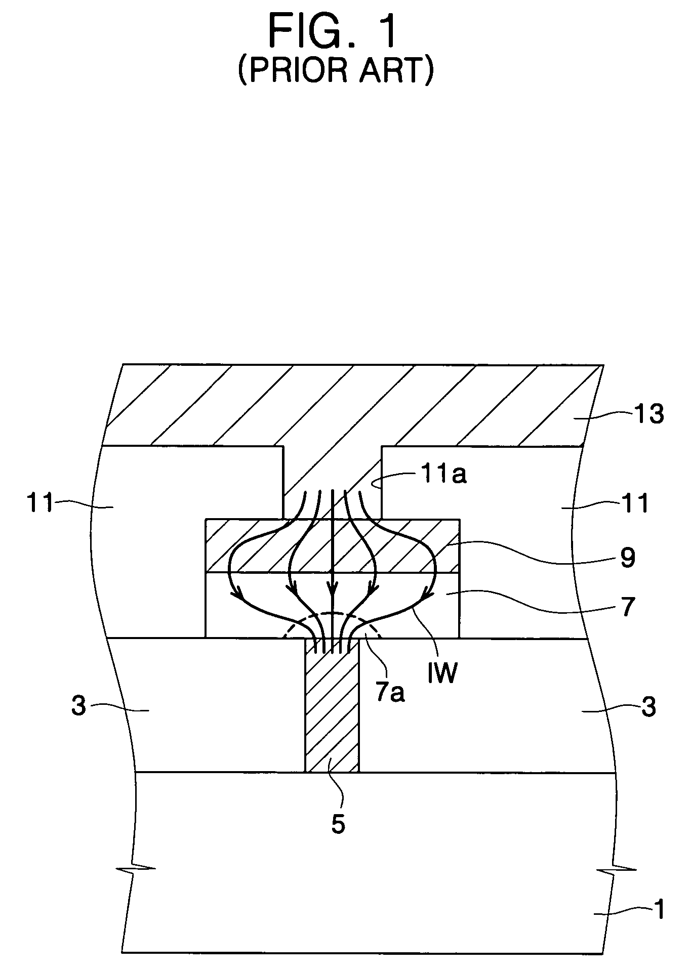
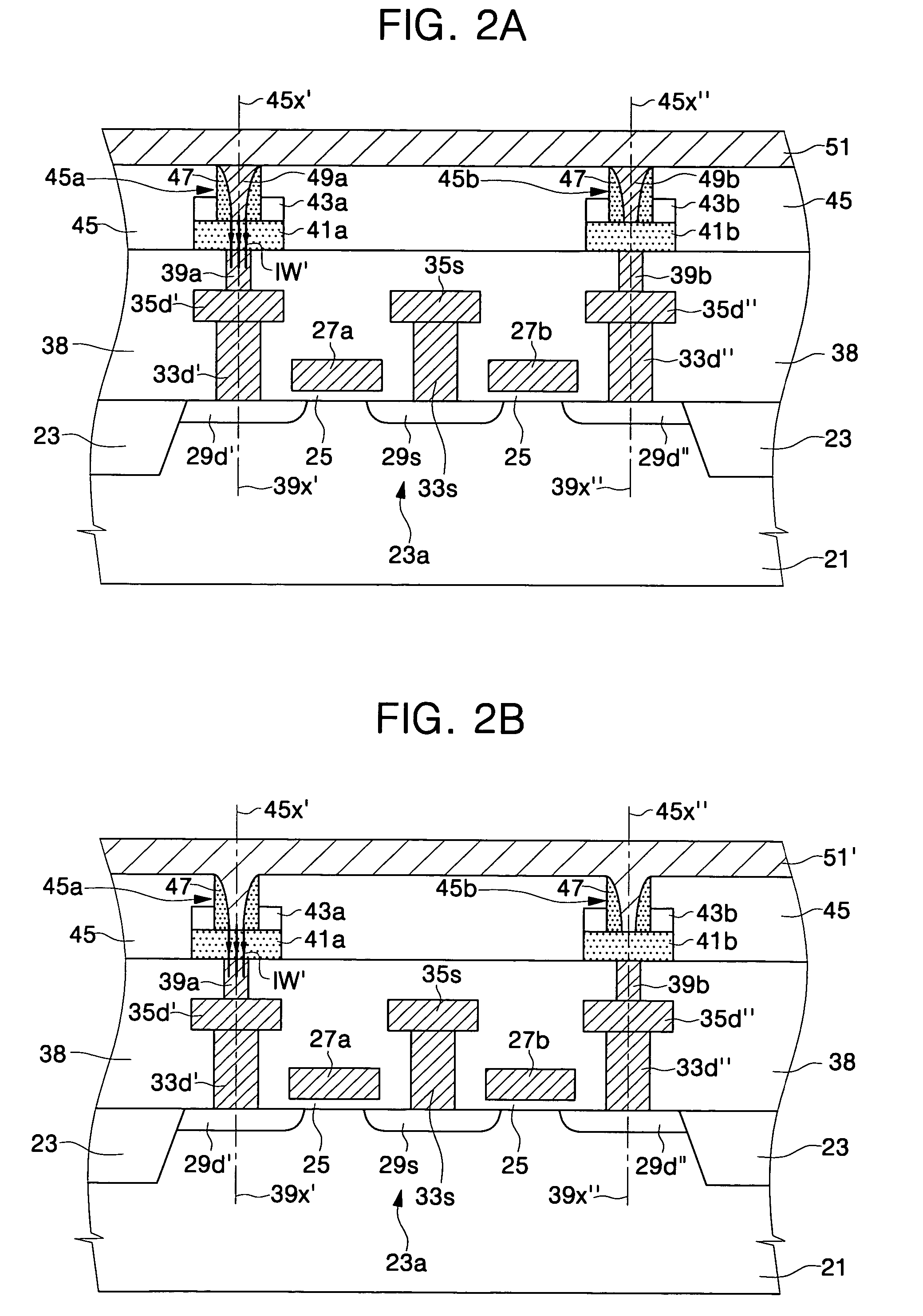
[0076]FIG. 9 is a graph showing the writing characteristics (program characteristics) of data storage elements according to the conventional art and an exemplary embodiment of the present invention. In FIG. 9, a horizontal axis denotes a writing voltage VW which is applied between an upper conductive plug and a lower conductive plug of each of the data storage elements, and a vertical axis denotes an electrical resistance R of each of the data storage elements. Also, in FIG. 9, data indicated by a reference numeral 101 corresponds to the program characteristics of the conventional data storage element, and data indicated by a reference numeral 103 corresponds to the program characteristics of the data storage element of an exemplary embodiment of the present invention.

[0077] The data storage elements exhibiting the measurement results of FIG. 9 were fabricated using the process conditions described in the following Table.

TABLEConventional ArtPresent InventionLower conductive plug...


PUM


Abstract

A phase changeable memory cell is provided. The phase changeable memory cell includes a lower interlayer dielectric layer formed on a semiconductor substrate and a lower conductive plug passing through the lower interlayer dielectric layer. The lower conductive plug is in contact with a phase change material pattern disposed on the lower interlayer dielectric layer. The phase change material pattern and the lower interlayer dielectric layer are covered with an upper interlayer dielectric layer. The phase change material pattern is in direct contact with a conductive layer pattern, which is disposed in a plate line contact hole passing through the upper interlayer dielectric layer. Methods of fabricating the phase changeable memory cell is also provided.

Description

[0001] This application claims the benefit of Korean Patent Application No. 10-2004-0101999, filed Dec. 6, 2004, the contents of which are hereby incorporated herein by reference in their entirety. BACKGROUND OF THE INVENTION [0002] 1. Field of the Invention [0003] The present invention relates to semiconductor devices and methods of forming the same and, more particularly, to phase changeable memory cells and methods of forming the same. [0004] 2. Description of Related Art [0005] Nonvolatile memory devices retain their stored data even when their power supplies are turned off and thus nonvolatile memory devices have been widely used in conjunction with computers, mobile telecommunication systems, memory cards and so on. For example, one widely used type of nonvolatile memory device is the flash memory device. Many flash memory devices employ memory cells having a stacked gate structure. The stacked gate structure of a flash memory device typically includes a tunnel oxide layer, a ...

Claims


Application Information

Patent Timeline
IPC IPC(8): H01L21/00H01L29/12
CPCH01L27/2436H01L45/06H01L45/122H01L45/1233H01L45/1273H01L45/144H01L45/1675H10B63/30H10N70/231H10N70/821H10N70/8418H10N70/826H10N70/8828H10N70/063H01L29/8615H10B63/00H10B99/00
Inventor YI, JI-HYECHO, BYEONG-OKCHO, SUNG-LAE
Owner SAMSUNG ELECTRONICS CO LTD
Why Eureka
Try Eureka