Semiconductor device including current control circuit of reference current source

Inactive Publication Date: 2006-06-08
KK TOSHIBA
View PDF16 Cites 19 Cited by
  • Summary
  • Abstract
  • Description
  • Claims
  • Application Information

AI Technical Summary

Benefits of technology

[0008] According to one embodiment of the present invention, there is provided a semiconductor device having a current control circuit comprises: a current source; a capacitor charged by the current output from the current source; a switch circuit for controlling charge and discharge of the capacitor; a voltage comparator for comparing the voltage o

Problems solved by technology

Accordingly, a problem arises in that a circuit margin must be set large by designing a reference current to a large value, and the like so that the settling characteristics satisfy a specification under all the conditions.
In this type of the circuit, however, since the stability of a system must be generally taken into consideration, the number of parameters such as the size of a transistor and the capacitance value of a capacitor to be selected, and the like, which must be taken into consideration in design, is increased, it is difficult to design a circuit to satisfy these parameters.

Method used


Image

  • Semiconductor device including current control circuit of reference current source
  • Semiconductor device including current control circuit of reference current source
  • Semiconductor device including current control circuit of reference current source

Examples


embodiment 1

[0017] A semiconductor device of this embodiment includes a current control circuit and a circuit to which a reference current is supplied from the current control circuit. The current control circuit will be described below in detail.

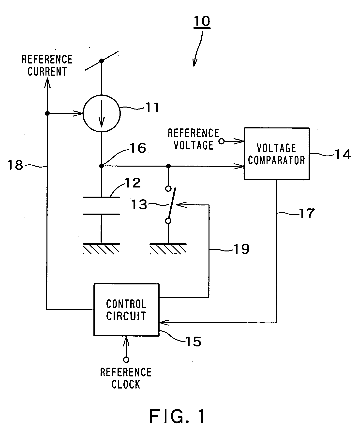
[0018]FIG. 1 is a block diagram showing a current control circuit of the embodiment 1 of the semiconductor device according to the present invention.

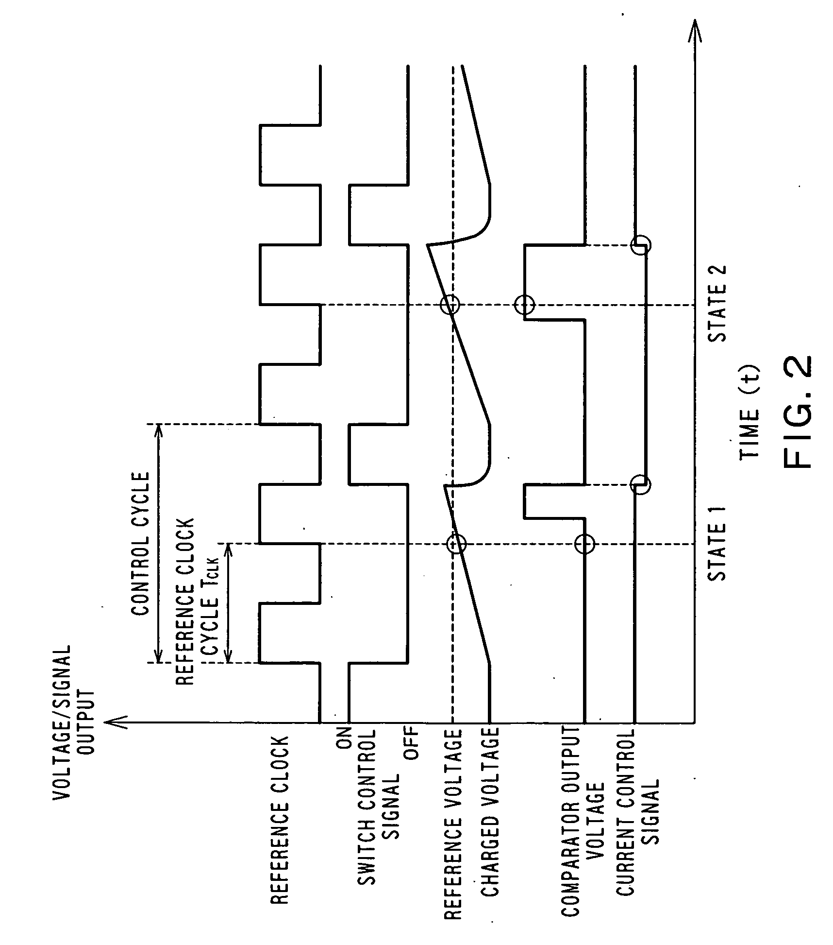
[0019] The current control circuit 10 has a current source 11, a capacitor 12 for accumulating a current from the current source 11, a switch circuit 13 for manipulating charge and discharge of the capacitor 12, a voltage comparator 14 for comparing the voltage of the capacitor 12 at a node 16 with the reference voltage from a reference voltage source (not shown) and outputting a result of comparison to a control circuit 15, and the control circuit 15 for controlling the current source 11 and the switch circuit 13. On receiving the output signal from the voltage comparator 14, the control circuit 15 outp...

embodiment 2

[0030] A semiconductor device of this embodiment includes a current control circuit and a circuit to which a reference current is supplied from the current control circuit. The current control circuit will be described below in detail.

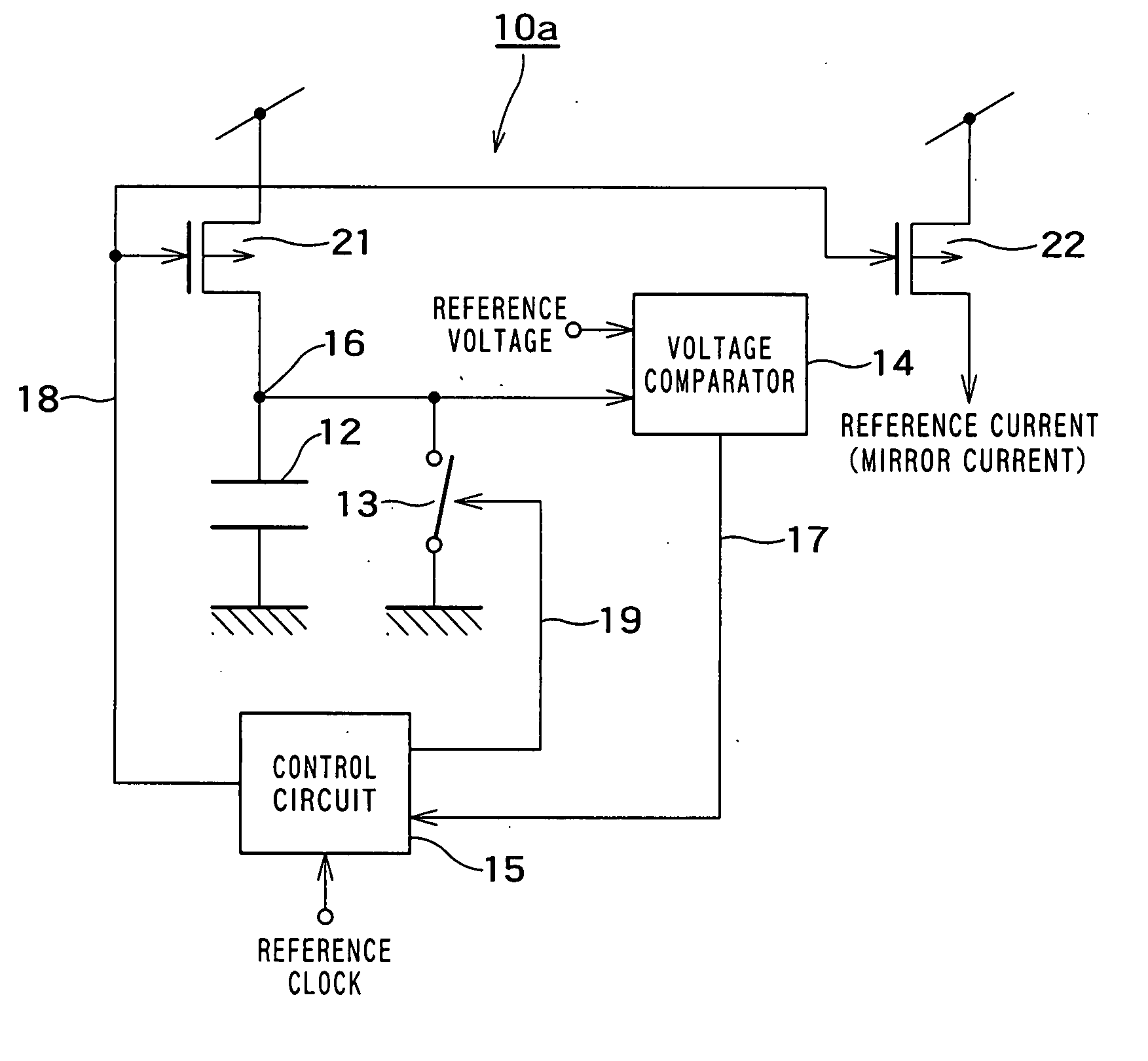
[0031]FIG. 3 is a block diagram showing a current control circuit of the embodiment 2 of the semiconductor device according to the present invention. The current control circuit of this embodiment has substantially the same basic configuration as the current control circuit of the embodiment 1.

[0032] The embodiment 2 is different from the embodiment 1 in that it employs a MOS transistor as a current source.

[0033] The current control circuit 10a has a first MOS transistor 21 as a current source, a capacitor 12 for accumulating a current from the first MOS transistor 21, a switch circuit 13 for manipulating charge and discharge of the capacitor 12, a voltage comparator 14 for comparing the voltage of the capacitor 12 at a node 16 with the reference vo...

embodiment 3

[0042] A semiconductor device of this embodiment includes a current control circuit and a circuit to which a reference current is supplied from the current control circuit. The current control circuit will be described below in detail.

[0043]FIG. 4 is a block diagram showing a current control circuit of the embodiment 3 of the semiconductor device according to the present invention. The current control circuit of this embodiment has substantially the same basic configuration as the current control circuit of the embodiment 2.

[0044] The embodiment 3 is different from the embodiment 2 in that a voltage D / A converter is disposed behind a control circuit.

[0045] The current control circuit 10b has a first MOS transistor 21 as a current source, a capacitor 12 for accumulating a current from the first MOS transistor 21, a switch circuit 13 for manipulating charge and discharge of the capacitor 12, a voltage comparator 14 for comparing the voltage of the capacitor 12 at a node 16 with the...


PUM


Abstract

A semiconductor device having a current control circuit includes: a current source; a capacitor charged by the current output from the current source; a switch circuit for controlling charge and discharge of the capacitor; a voltage comparator for comparing the voltage of the charged capacitor with a reference voltage; and a control circuit for creating a control signal based on a result of comparison, feeding back the control signal to the current source so that the voltage of the capacitor is made near to the reference voltage as well as controlling a reference current output to the outside by the control signal.

Description

CROSS REFERENCE TO RELATED APPLICATION [0001] This application is based upon and claims the benefit of priority from the prior Japanese Patent Application No. 2004-318894, filed on Nov. 2, 2004; the eitire contents of which are incorporated herein by reference. BACKGROUND OF THE INVENTION [0002] 1. Field of the Invention [0003] The present invention relates to a semiconductor device including a current control circuit of a reference current source. [0004] 2. Related Background Art [0005] Heretofore, in a general analog circuit including a circuit such as a switched-capacitor circuit and the like for charging and discharging a capacitor, a reference current source for determining the operation current of the overall circuit is designed to have a constant current value. In this case, the settling characteristics of the switched-capacitor circuit have such a factor that they are varied depending on the change of a clock cycle, the manufacturing dispersion of the capacitance value of a ...

Claims


Application Information

Patent Timeline
IPC IPC(8): G05F1/10
CPCG05F3/262
Inventor SAKURAI, SATOSHIDOBASHI, NORIAKI
Owner KK TOSHIBA
Why Eureka
Try Eureka