PCI Express Physical Layer Built-In Self Test Architecture

a self-testing and physical layer technology, applied in error detection/correction, instruments, digital transmission, etc., can solve the problems of b>100/b>, built-in self-test circuit, and inability to predict the loopback latency,

Active Publication Date: 2006-06-08
VIA LABS INC
View PDF3 Cites 14 Cited by
  • Summary
  • Abstract
  • Description
  • Claims
  • Application Information

AI Technical Summary

Problems solved by technology

However, the lane under test 110 of the PCI Express includes a plurality of loopback paths, which also means that time required by the test patterns to pass through the lane under test 110 is not constant, so that the loopback latency cannot be predicted.
Furthermore, the built-in self test circuit architecture 100 will be affected by phase jitter which causes errors in the pattern comparison module 108.
Moreover, the storage capacity of the pattern register 106 must be restricted; therefore when the loopback latency becomes too great, the built-in self test architecture 100 will not operate accurately.

Method used


Image

  • PCI Express Physical Layer Built-In Self Test Architecture
  • PCI Express Physical Layer Built-In Self Test Architecture
  • PCI Express Physical Layer Built-In Self Test Architecture

Examples


Embodiment Construction

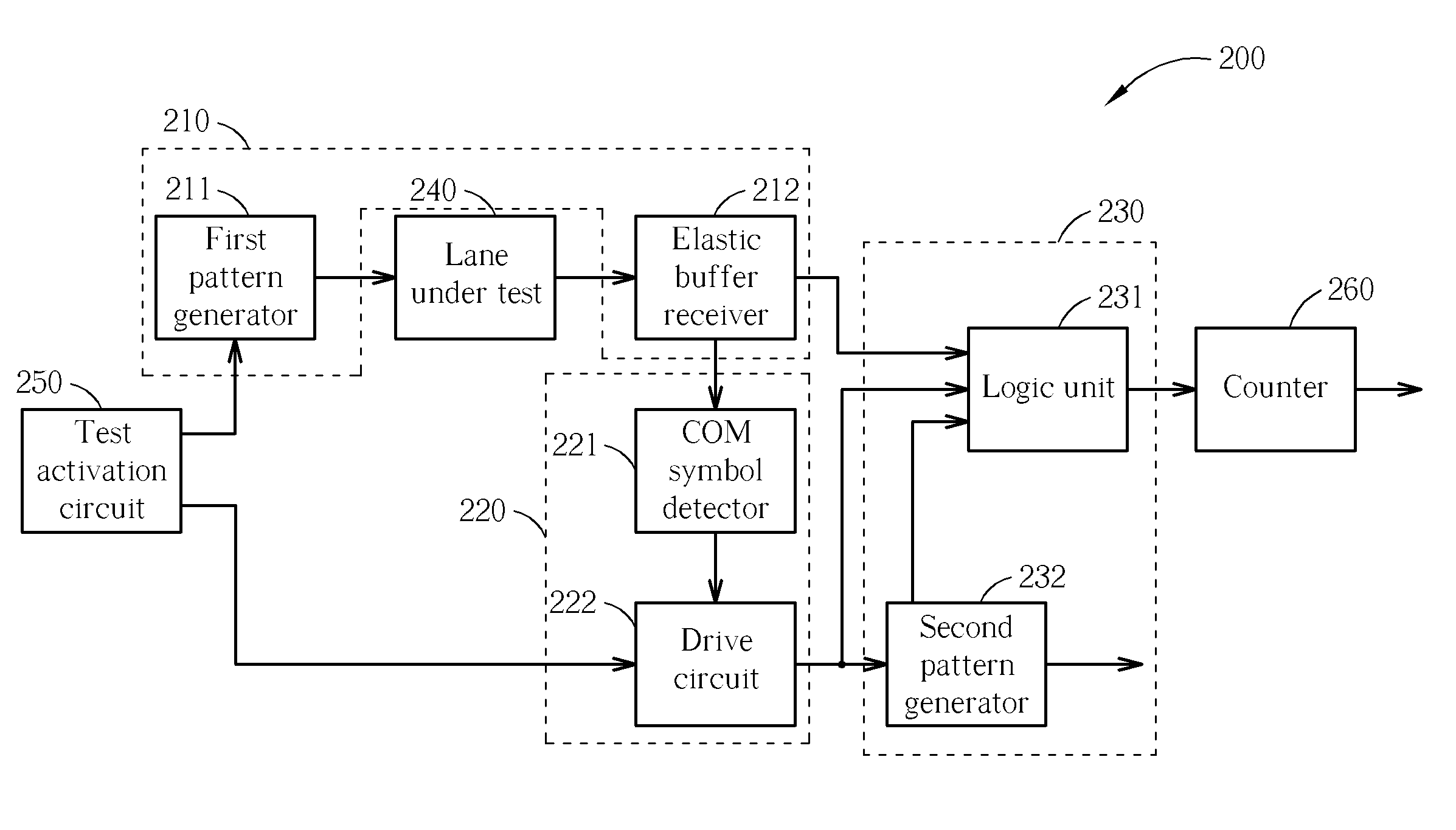
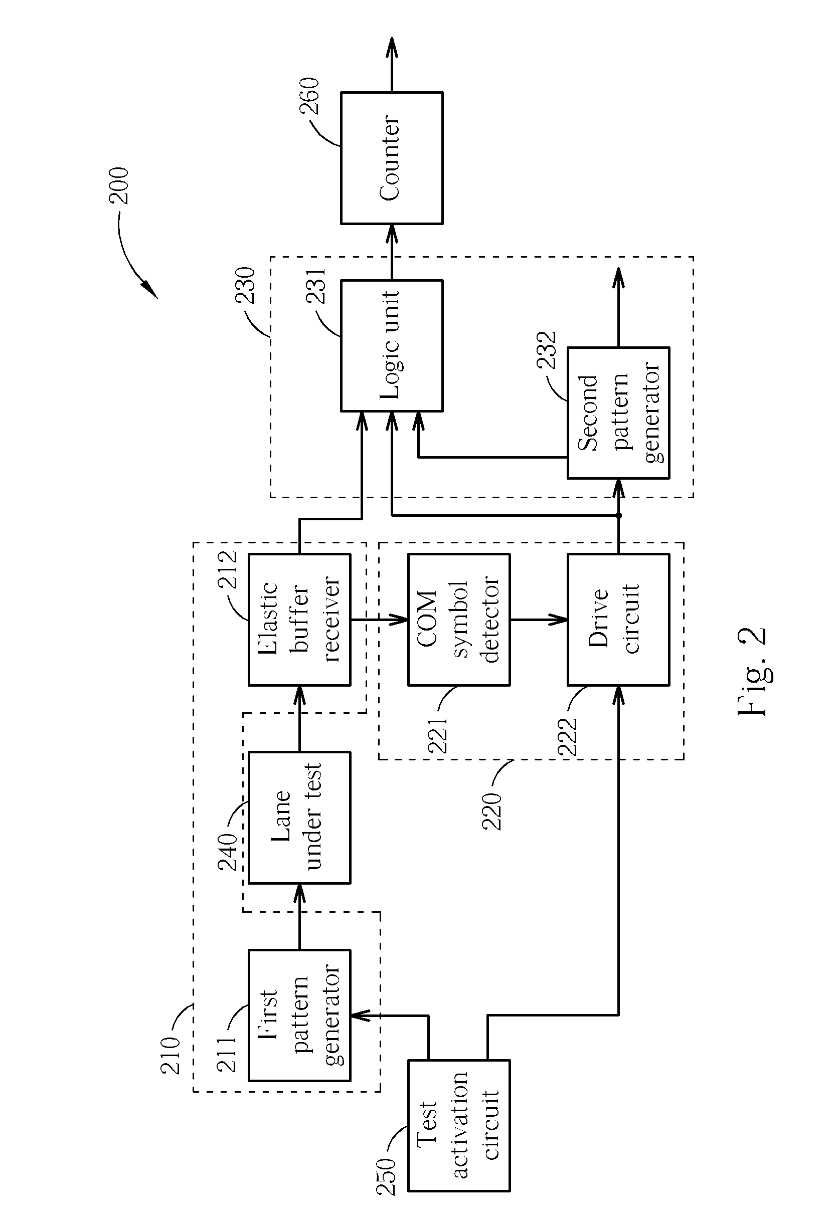
[0016] Please refer to FIG. 2. FIG. 2 illustrates a diagram of a PCI Express physical layer built-in test circuit architecture 200. The architecture 200 is capable of compensating loopback latency of the PCI Express, wherein the architecture 200 includes a test unit 210, a detecting unit 220, and a compare unit 230. The test unit 210 includes a first pattern generator 211 and an elastic buffer receiver 212. The detecting unit 220 includes a command (COM) symbol detector 221 and a drive circuit 222. The compare unit 230 includes a second pattern generator 232 and a logic unit 231. Furthermore, the built-in self test circuit 200 further includes a test activation circuit 250 and a counter 260. In FIG. 2, a lane under test 240 is a lane in the PCI Express physical layer required to be tested. The operating method of the built-in self test circuit architecture 200 will be explained in the following.

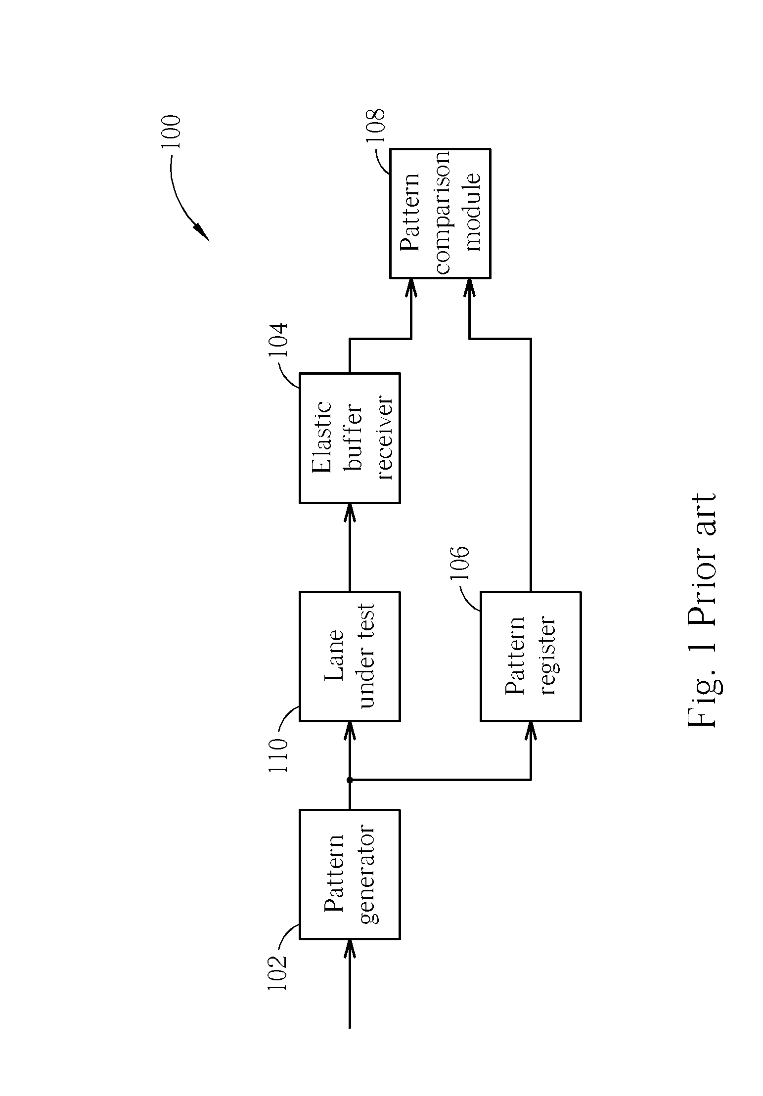
[0017] According to the standards of the PCI Express, each sequence symbol transmitted b...


PUM


Abstract

A built-in self test circuit includes a first pattern generator, an elastic buffer receiver, a command symbol detector, a second pattern generator, and a logic unit. The architecture is capable of compensating loopback latency automatically without having to utilize a device that stores test patterns generated by the first pattern generator, and error warning can be greatly reduced. Also, the architecture can reduce the effect of phase jitter and error rate count is provided. Hence, accuracy of test can be increased.

Description

CROSS REFERENCE TO RELATED APPLICATIONS [0001] This application claims the benefit of U.S. Provisional Application No. 60 / 522,812, filed 11 / 09 / 2004, and included herein by reference. BACKGROUND OF THE INVENTION [0002] b 1. Field of the Invention [0003] The present invention relates to a built-in test circuit, more particularly a PCI Express physical layer built-in test circuit capable of detecting command symbols to automatically compensate loopback latency. [0004] 2. Description of the Prior Art [0005] In the development of personal computer systems and peripheral devices, bandwidth and speed requirements of the interconnect interface are increasing. The load of a conventional PCI device becomes greater, therefore the third generation input / output (3GIO) has gradually replaced PCI interface to provide the greater bandwidth requirement. The third generation input / output (3GIO) is also known as a PCI Express interface. Those skilled in the arts know that the PCI Express technology ut...

Claims


Application Information

Patent Timeline
Patent Type & Authority Applications(United States)
IPC IPC(8): G01R31/28G06F11/22G06F13/40H04L1/24
CPCG06F11/27H04L25/03866
Inventor TSENG, WAYNE
Owner VIA LABS INC
Why Eureka
Try Eureka