Circuit and method for detecting pixel defect

a technology of defect detection and circuit, applied in the field of imaging devices, can solve the problems of increased production cost, new pixel defect due to ageing deterioration, unreachable, etc., and achieve the effects of high-accuracy pixel defect detection, low cost circuitry, and simple circuitry

Inactive Publication Date: 2006-06-15
SONY CORP
View PDF2 Cites 18 Cited by
  • Summary
  • Abstract
  • Description
  • Claims
  • Application Information

AI Technical Summary

Benefits of technology

[0013] According to an embodiment of the present invention, therefore, first, pixel signals on one horizontal line are input from an imaging device, and, then, a level of a target pixel signal is compared with levels of a plurality of surrounding pixel signals located to the right and left of the target pixel signal. If a difference between the levels is higher than a threshold value, the pixel corresponding to the target pixel signal is detected as a possible defective pixel, and the address of the detected possible defective pixel is held. After holding the levels of the detected possible defective pixel signal and the surrounding pixel signals from the pixel signals in the next frame, a correlation between the possible defective pixel signal and the surrounding pixel signals is calculated. If the correlation is not found, the possible defective pixel is detected as a pseudo-defective pixel, and the detection of the pseudo-defective pixel is performed for a predetermined number of frames. If the number of times the pseudo-defective pixel has been detected is equal to the predetermined number of frames, the pseudo-defective pixel is detected as a true defective pixel. A line memory having a capacity for holding at least one horizontal line of pixel signals, and a memory having a capacity for holding at least an address of a possible defective pixel and signal levels of, for example, nine pixel signals including a possible defective pixel signal and surrounding pixel signals of the possible defective pixel signal are needed. It is therefore possible to detect pixel defects of an imaging device with simple, low-cost circuitry. Moreover, three detection steps of detecting a possible defective pixel, detecting a pseudo-defective pixel, and detecting a true defective pixel allow high-accuracy detection of pixel defects.

Problems solved by technology

However, the former method needs an inspection step of illuminating an imaging device with uniform illumination at the time of inspection during manufacturing, and the production cost therefore increases.
Furthermore, a new pixel defect due to aged deterioration after the product is delivered to the customer is not addressed because the address of the defective pixel is not stored in the EEPROM.
Moreover, an expensive memory, such as an EEPROM, is not needed.
Thus, the complexity of the circuit arrangement increases.

Method used


Image

  • Circuit and method for detecting pixel defect
  • Circuit and method for detecting pixel defect
  • Circuit and method for detecting pixel defect

Examples


Embodiment Construction

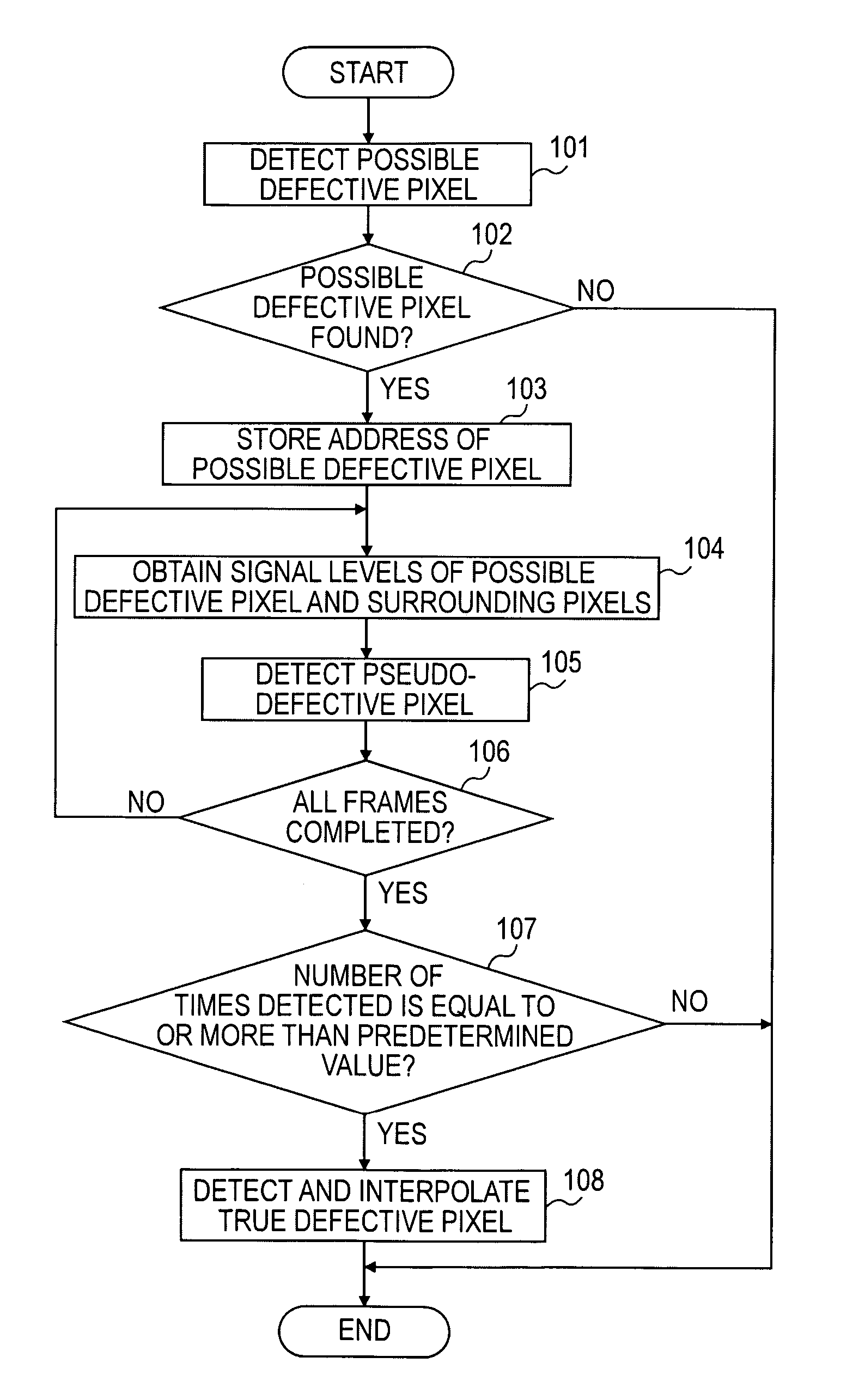
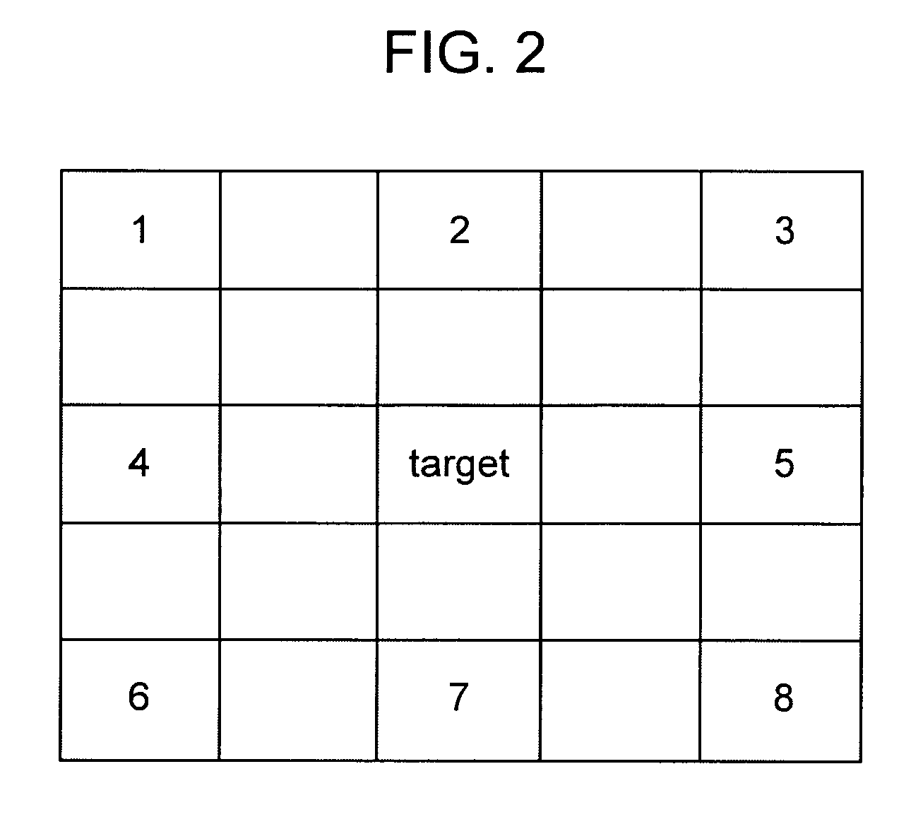
[0017] A pixel defect of an imaging device is automatically detected with simple, low-cost circuitry in the following way. Pixel signals on one horizontal line are input from the imaging device, and a level of a target pixel signal is compared with levels of a plurality of surrounding pixel signals located to the right and left of the target pixel signal. If a difference between the levels is higher than a threshold value, the pixel corresponding to the target pixel signal is detected as a possible defective pixel, and the address of the detected possible defective pixel is held. After holding the levels of the detected possible defective pixel signal and the surrounding pixel signals from the pixel signals in the next frame, a correlation between the possible defective pixel signal and the surrounding pixel signals is calculated. If the correlation is not found, the possible defective pixel is detected as a pseudo-defective pixel, and the detection of the pseudo-defective pixel is ...


PUM


Abstract

A circuit for detecting a pixel defect includes the following elements. A first defect detector compares a level of a target pixel signal on one horizontal pixel signal line of pixel signals input from an imaging device with levels of a plurality of surrounding pixel signals of the target pixel signal to determine whether or not a pixel corresponding to the target pixel signal is a possible defective pixel according to a comparison result. A second defect detector calculates a correlation between the detected possible defective pixel signal and the surrounding pixel signals to determines whether or not the possible defective pixel is a pseudo-defective pixel. A third defect detector performs the detection of the detected possible defective pixel on pixel signals in a predetermined number of frames, and determines that the pseudo-defective pixel is a true defective pixel when the pseudo-defective pixel is detected in all frames.

Description

CROSS REFERENCES TO RELATED APPLICATIONS [0001] The present invention contains subject matter related to Japanese Patent Application JP 2004-356473 filed in the Japanese Patent Office on Dec. 9, 2004, the entire contents of which are incorporated herein by reference. BACKGROUND OF THE INVENTION [0002] 1. Field of the Invention [0003] The present invention relates to imaging devices. More specifically, the present invention relates to a pixel defect detecting circuit and method for use in solid-state imaging devices, such as charge-coupled devices (CCDs), for detecting pixel defects. [0004] 2. Description of the Related Art [0005] Solid-state imaging devices, such as CCDs, typically detect and correct for image display errors, such as white defects. A white defect occurs such that a video signal region having a high signal level due to a crystal defect of a semiconductor device causes a higher brightness than an image portion therearound to bring a white pixel condition. [0006] In a ...

Claims


Application Information

Patent Timeline
Patent Type & Authority Applications(United States)
IPC IPC(8): H04N5/217H04N9/64G06T1/00H04N1/40H04N5/335H04N5/367H04N5/369H04N5/372
CPCH04N5/3675H04N9/646H04N25/683
Inventor YONEDA, MASATO
Owner SONY CORP
Why Eureka
Try Eureka