Memory device and electronic device using the same

a memory device and electronic device technology, applied in the field of memory devices, can solve the problems of low security level, limited storage capacity of smart cards, enlargement of information capacity, etc., and achieve the effects of low cost, large storage capacity, and high security level

Inactive Publication Date: 2006-06-15
PANASONIC CORP
View PDF3 Cites 110 Cited by
  • Summary
  • Abstract
  • Description
  • Claims
  • Application Information

AI Technical Summary

Benefits of technology

[0015] The secure area cannot directly be accessed by an external device and therefore has the higher security level than the authentication area in the related art. Moreover, since the secure area is placed in the non-tamper-resistant memory, a large storage capacity can be reserved at a low cost.

Problems solved by technology

However, the Smart card has a limited storable information capacity and enlargement of the information capacity is demanded by service providers, etc., with diversification of digital cash service.
However, the authentication area is an area that can be controlled directly by an external device and therefore the security level is low as compared with the Smart card.

Method used


Image

  • Memory device and electronic device using the same
  • Memory device and electronic device using the same
  • Memory device and electronic device using the same

Examples


Embodiment Construction

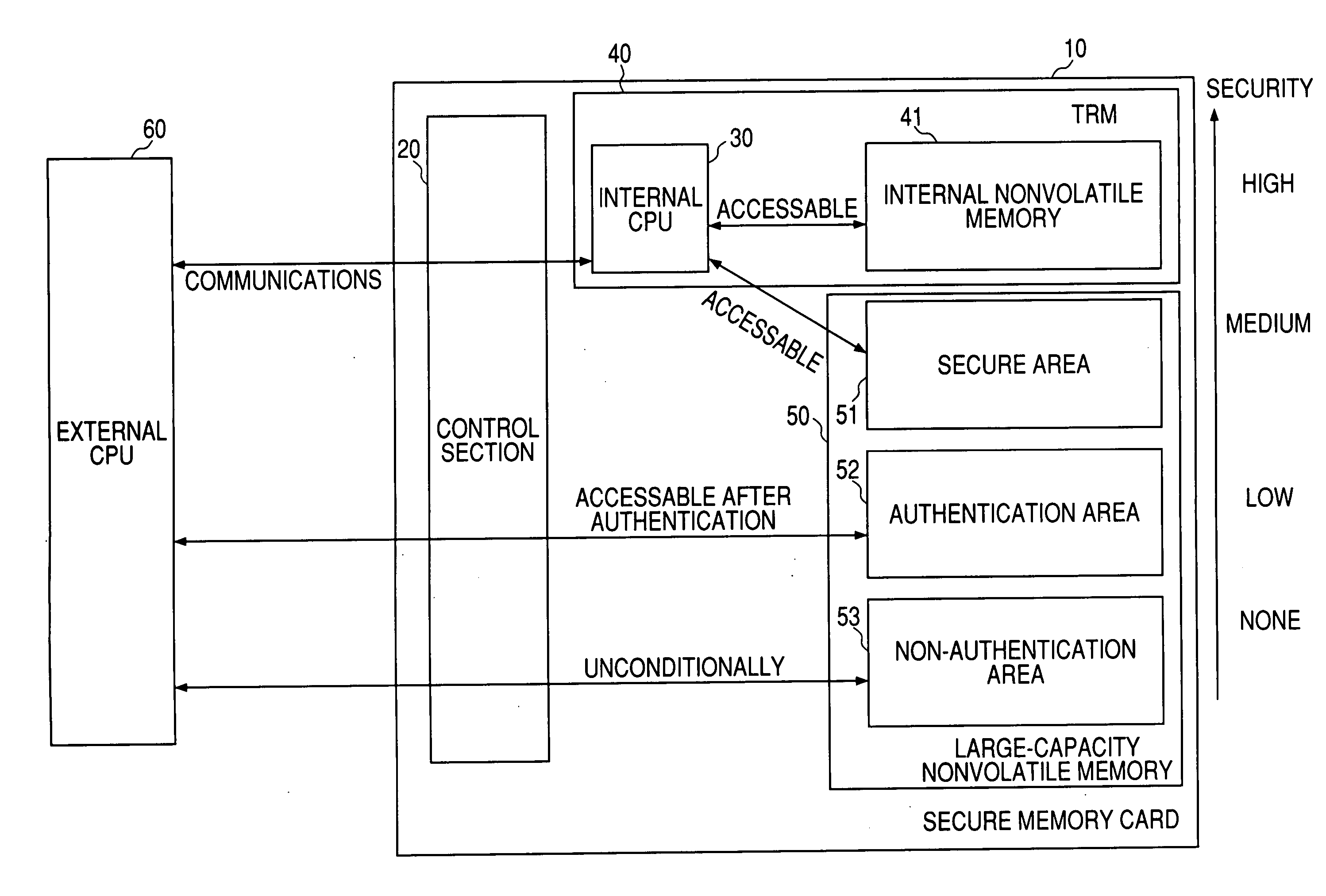
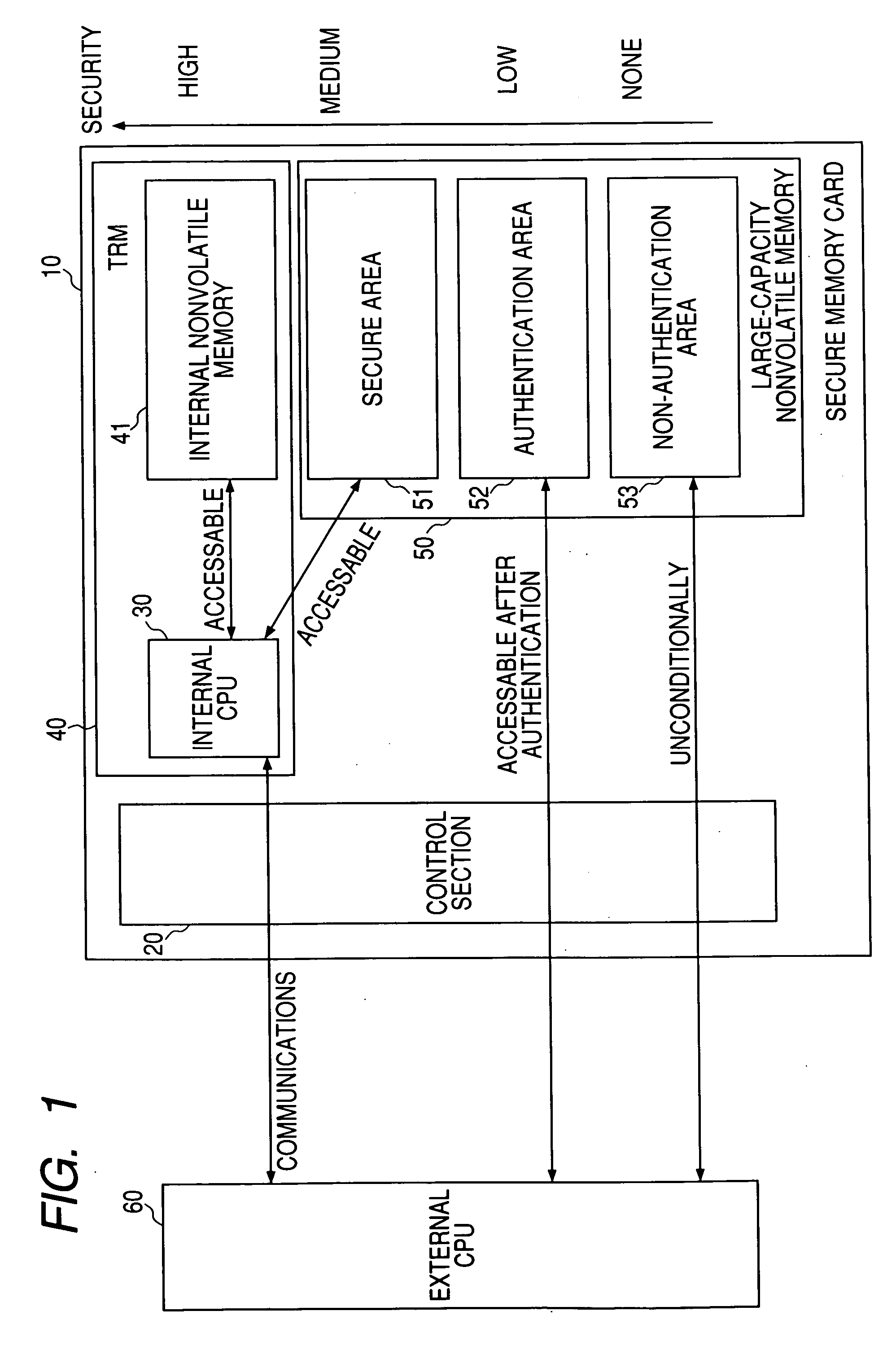
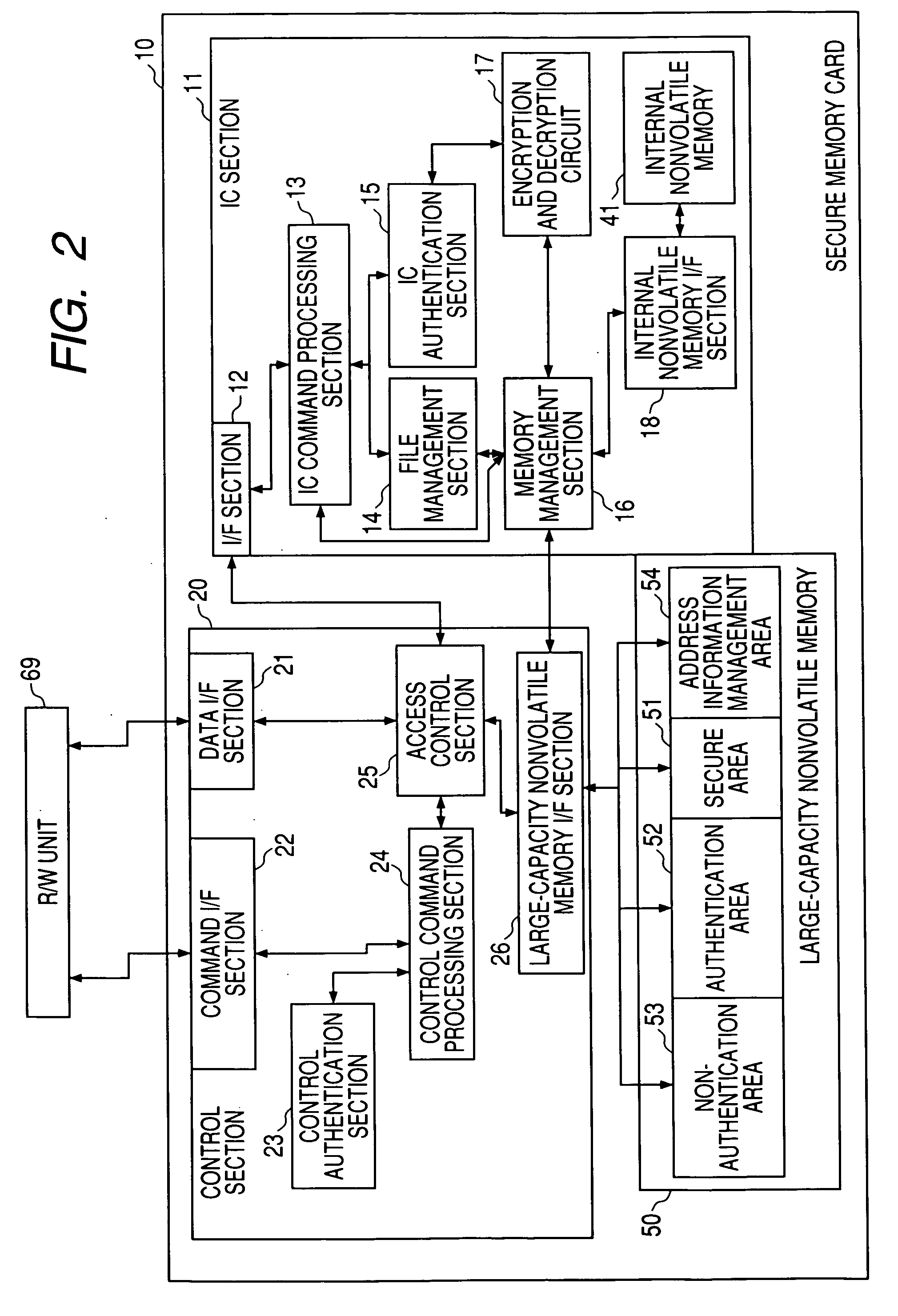
[0031] A semiconductor memory card in an embodiment of the invention (here, called “secure memory card”) comprises a tamper-resistant module (TRM) 40 including internal nonvolatile memory 41, large-capacity nonvolatile memory 50 including a non-authentication area 53, an authentication area 52, and a secure area 51, an internal CPU 30 for accessing the internal nonvolatile memory 41 and the secure area 51, and a control section 20 for communicating with an external CPU 60 of an electronic device (read / write (R / W) unit) to perform authentication processing and permitting the authenticated external CPU 60 to access the authentication area 52, as shown in a conceptual drawing of FIG. 1.

[0032] The nonvolatile memory 41 of the TRM 40 is implemented as EEPROM that can be erased and written in 16-byte units, for example. The large-capacity nonvolatile memory 50 is implemented as flash memory that can be erased in block units of 16 K bytes, etc., and can be written in 512-bytes units, for ...


PUM


Abstract

It is an object of the invention to provide a memory device including a memory area having a large storage capacity and an equal security level to that of a Smart card.
A semiconductor memory card 10 that can be attached to and detached from an electronic device is provided with first memory 50 of non-tamper-resistance having usual areas 52 and 53 that can be accessed from the electronic device and a secure area 51 that cannot directly be accessed from the electronic device, and second memory 41 of tamper resistance that cannot directly be accessed from the electronic device, wherein access to the secure area 51 of the first memory 50 can be made only through a secure control section 30 for managing access to the second memory 41. The secure area 51 cannot directly be accessed by an external device and therefore has the higher security level than the authentication area 52. Since the secure area 51 is placed in the non-tamper-resistant memory 50, a large storage capacity can be reserved.

Description

TECHNICAL FIELD [0001] This invention relates to a memory device such as a semiconductor memory card and an electronic device for writing / reading data into / from the memory device, and in particular to implementation of a storage medium assuring a high level of security and having a large storage capacity. BACKGROUND ART [0002] A semiconductor memory card including nonvolatile semiconductor memory as a storage medium, (which will be hereinafter referred to as “memory card”), has a small storage capacity as compared with a disc-like storage medium such as a DVD, but does not require a large mechanical section and is small and easy to handle and is also excellent in earthquake resistance and therefore recently has had the use range expanded as a storage medium fitted for portable use. [0003] The memory card may or may not contain a CPU (microcomputer). The function of the CPU in the memory card containing the CPU is to perform nonvolatile memory read and write processing requested by a...

Claims


Application Information

Patent Timeline
Patent Type & Authority Applications(United States)
IPC IPC(8): G11C8/02G06F12/14G06F21/10G06F21/60G06F21/62G06F21/75G06F21/86G06K19/073G06K19/10G07F7/08G11C5/00H04L9/08H04L9/10
CPCG06F12/1433G06Q20/32G11C5/005G07F7/0866G06Q20/363G06Q20/326G06F12/14G06K19/073
Inventor TAKAGI, YOSHIHIKONAKANISHI, YOSHIAKISAKAKI, OSAMUKIKUCHI, TAKAFUMI
Owner PANASONIC CORP
Why Eureka
Try Eureka