Rewritable nano-surface organic electrical bistable devices

a nano-surface organic electrical and bistable technology, applied in thermoelectric devices, solid-state devices, nano-informatics, etc., can solve the problems of complex architecture, reduced electroluminescence of doped polymers, and relatively long time-consuming dipole group rotation, etc., to achieve high memory performance

Inactive Publication Date: 2006-06-22
RGT UNIV OF CALIFORNIA
View PDF44 Cites 14 Cited by
  • Summary
  • Abstract
  • Description
  • Claims
  • Application Information

AI Technical Summary

Benefits of technology

[0014] In accordance with the present invention, bistable electrical devices are provided that are convertible between a low resistance (impedance) state and a high resistance (impedance) state. The bistable electrical devices are well suited for use as electrical switching and memory devices. In the present invention, we provide a new kind of organic bistable device (OBD) that utilizes a nano-surface (also referred to as a “buffer layer”) located on at least one of the electrodes. The OBD's in accordance with the present invention provide high memory performance without any of the above-mentioned technical difficulties for memory applications.
[0015] The organic bistable electrical devices of the present invention generally include a first electrode that has a first electrode surface. A layer of low conductivity organic material having a first surface and a second surface is provided wherein the first surface of the organic layer is in electrical contact with the first electrode surface. A second electrode is provided that includes a second electrode surface. As a feature of the invention, a buffer layer is located between the second electrode surface and the second surface of organic layer. The buffer layer includes particles in the form of flakes or dots of a low conducting material or insulating material that are present in a sufficient amount to only partially cover the second electrode surface. The buffer layer controls metal ion migration from the electrode and provides for the conversion of the bistable electrical device between the low resistance (“on”) state and the high resistance (“off”) state when an electrical voltage is applied between the first and second electrodes.
[0016] The present invention utilizes one or more buffer layers to control the metal ion concentration within the organic layer interposed between two metal electrodes and provide electrical programmable nonvolatile memory devices. Advantages of the memory devices of the present invention include: 1) the memory devices have no conducting layer in between the top and bottom electrodes. Therefore, it is not necessary to pattern the active layer (which is composed of one or more buffer-layers and organic layers) when making x-y memory-cell array type memory devices; 2) the write-read-erase voltage pulse can be the same direction, which is convenient in an x-y electrical-addressable memory array device. This is because in x-y array type devices, a diode must be series connected with each memory cell to prevent the sneak current. In addition, the on-state current is much higher, at 0.1 V bias, the on-state current can go to 2 A / cm2. Both the On-state and Off-state are quite stable. As a result, this device is ideal for x-y array type memory and switch application.

Problems solved by technology

Unfortunately, rotation of the dipole groups takes a relatively long time.
Also, doping of the polymer reduces the electroluminescence of the doped polymer.
Although these inorganic devices have been technically and commercially successful, they have a number of drawbacks including complex architecture and high fabrication costs.
This results in heating and high power consumption.
However, they have the disadvantage of reduced data storage capability as a result of higher complexity in the circuit design, and hence higher cost.
However such organic memories require transistor switches to address each memory element leading to a very complex device structure.
In this type of application, it is difficult to apply a reversed bias for erasing.
In addition, the middle metal layer makes it technically difficult to pattern the metal layer for each memory cell when the cells are very small.
The diffusion or drift of Cu-ions into semiconductor materials, like silicon, is a well-known and troublesome phenomenon that has an adverse effect on semiconductor devices (16).

Method used


Image

  • Rewritable nano-surface organic electrical bistable devices
  • Rewritable nano-surface organic electrical bistable devices
  • Rewritable nano-surface organic electrical bistable devices

Examples


Embodiment Construction

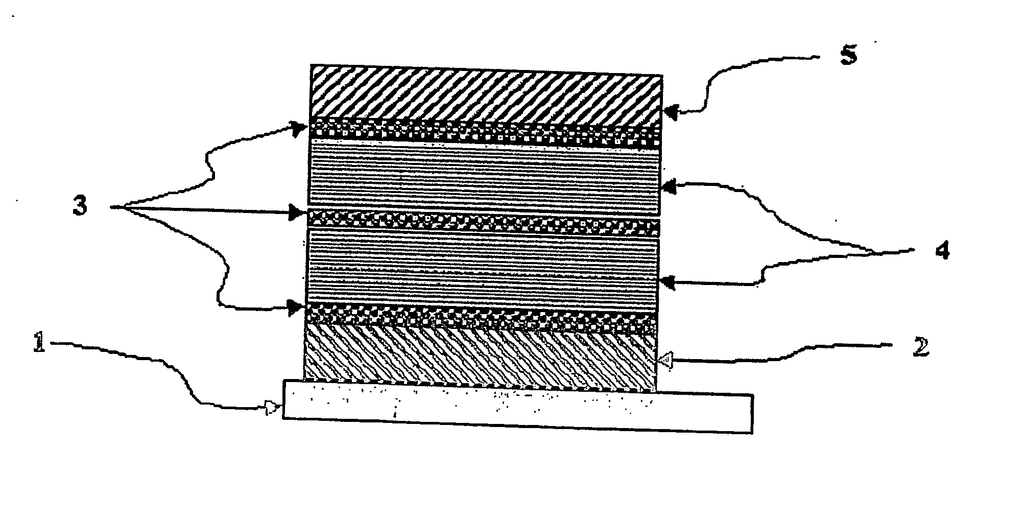
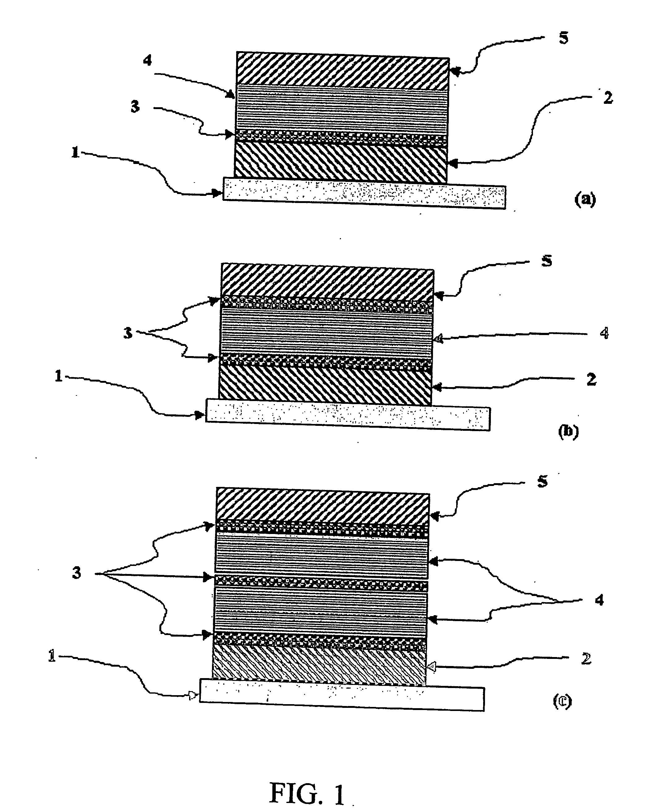
[0042] An organic bistable electrical device in accordance with the present invention is shown in FIG. 1. The device includes an organic layer 4 that is sandwiched between a first electrode 5 and a second electrode 2. The organic layer 4 is shown in the form of a layer. However, it will be understood that the organic layer can be provided in any number of different shapes. Organic layers in the form of a thin layer or film are preferred since fabrication techniques for forming thin films are well known.

[0043] The organic layer 4 includes a first surface that is in electrical contact with the first electrode 5. The organic layer 4 includes a second surface that is located on the other side of the organic layer 4 and which is in electrical contact with the second electrode 2. The second electrode 2 is typically located on an insulating substrate 1. If desired, the substrate 1 can be either ridged or flexible and made from either organic or inorganic materials that are well-know for u...


PUM


Abstract

A bistable electrical device that is convertible between a low resistance state and a high resistance state. The device includes at least one layer of organic low conductivity material that is sandwiched between two electrodes. A buffer layer is located between the organic layer and at least one of the electrodes. The buffer layer includes particles in the form of flakes or dots of a low conducting material or insulating material that are present in a sufficient amount to only partially cover the electrode surface. The presence of the buffer layer controls metal migration into the organic layer when voltage pulses are applied between the electrodes to convert the device back and forth between the low and high resistance states.

Description

BACKGROUND OF THE INVENTION [0001] 1. Field of the Invention [0002] The present invention relates generally to electronic devices that utilize elements that exhibit bistable electrical behavior. More particularly, the present invention is directed to organic semiconductor devices including electrically programmable nonvolatile memory devices and switches. [0003] 2. Description of Related Art [0004] The publications and other reference materials referred to herein to describe the background of the invention and to provide additional details regarding its practice are hereby incorporated by reference. For convenience, the reference materials are numerically referenced and identified in the appended bibliography. [0005] Many electronic memory and switching devices typically employ some type of bistable element that can be converted between a high impedance state (off-state) and a low impedance state (on-state) by applying an electrical voltage or other type of writing input to the devi...

Claims


Application Information

Patent Timeline
Patent Type & Authority Applications(United States)
IPC IPC(8): H01L29/08H01L27/28H01L51/00H01L51/30
CPCB82Y10/00H01L27/28H01L51/0051H01L51/0067H01L51/0591H01L51/0595H10K19/00H10K85/611H10K85/654H10K10/701H10K10/50
Inventor YANG, YANGMA, LIPING
Owner RGT UNIV OF CALIFORNIA
Why Eureka
Try Eureka