Image sensor package, solid state imaging device, and fabrication methods thereof

a technology of image sensor and solid-state imaging, which is applied in the direction of semiconductor devices, semiconductor/solid-state device details, electrical apparatus, etc., can solve the problems of increasing production costs, affecting the quality of image sensor packages, and inability to be directly handled by users as electric devices, etc., and achieves the effect of reducing the number of fabrication processing steps

Inactive Publication Date: 2006-06-29
SAMSUNG ELECTRONICS CO LTD
View PDF1 Cites 14 Cited by
  • Summary
  • Abstract
  • Description
  • Claims
  • Application Information

AI Technical Summary

Benefits of technology

[0011] It is therefore an object of the present invention to provide a small and thin image sensor package through reduced fabrication processing steps, a solid state imaging device, and fabrication methods thereof.

Problems solved by technology

A semiconductor device fabricated on a wafer, e.g., a chip is fragile and therefore, cannot be directly handled by a user as an electric device.
Since a conventional image sensor package uses a wire bonding method to electrically connect the image sensor chip and the substrate, the size and thickness of the entire package becomes thick due to the loop height of the wire, and the production cost is increased as well.
Also, since the glass or the glass module is attached to each image sensor chip, the entire size of the image sensor package becomes large and the production cost is increased.

Method used


Image

  • Image sensor package, solid state imaging device, and fabrication methods thereof
  • Image sensor package, solid state imaging device, and fabrication methods thereof
  • Image sensor package, solid state imaging device, and fabrication methods thereof

Examples


Embodiment Construction

[0027] Certain embodiments of the present invention will next be described in greater detail with reference to the accompanying drawings. However, the present invention should not be construed as being limited thereto.

[0028] In the following description, the same drawing reference numerals are used to depict the same elements in the various drawings. The subject matter including a detailed construction and elements defined herein are provided to assist in a comprehensive understanding of the invention, and it is to be understood that the present invention can be carried out in other ways. Also, well-known functions or constructions are not described in detail since they would obscure the invention in unnecessary detail.

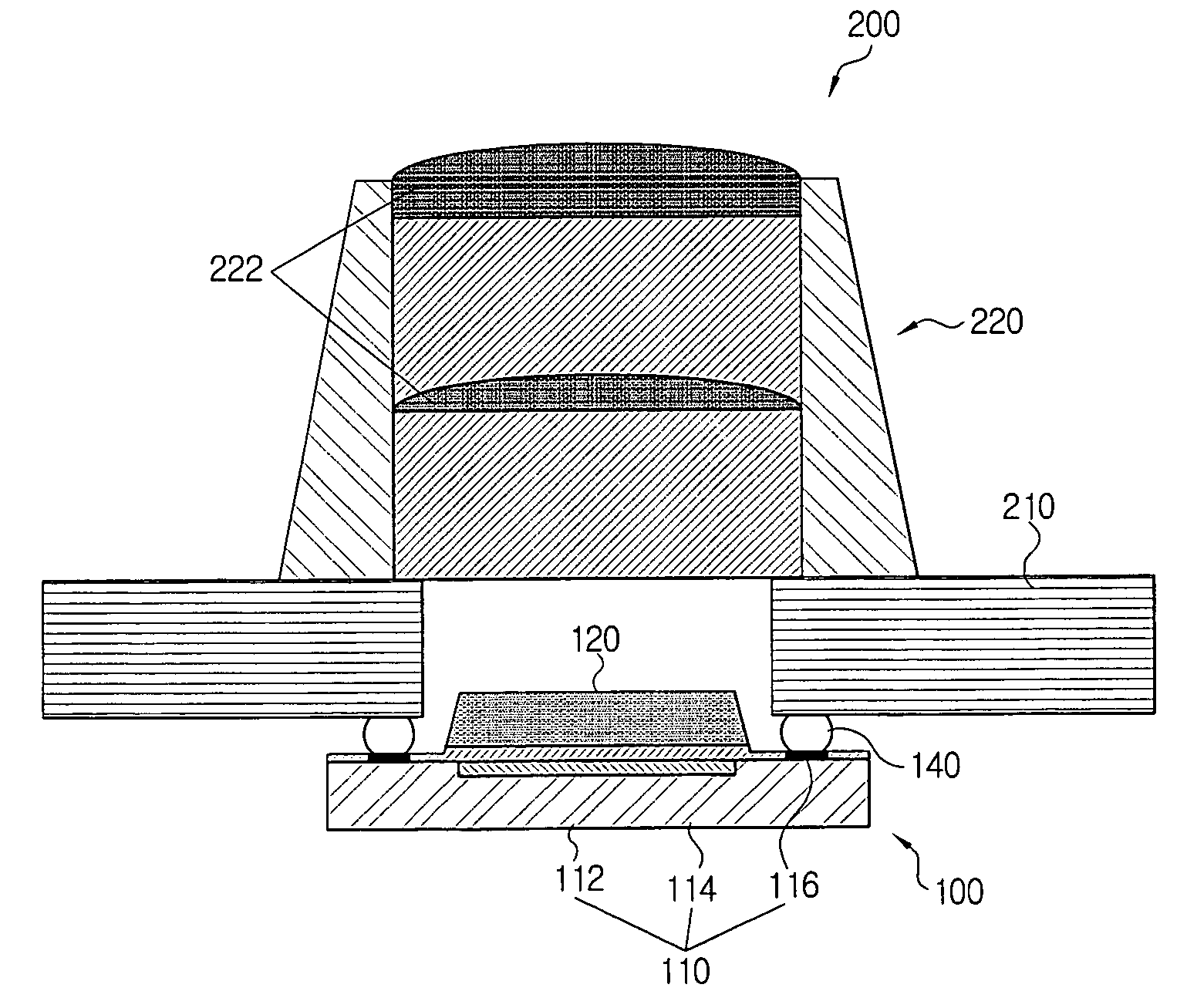
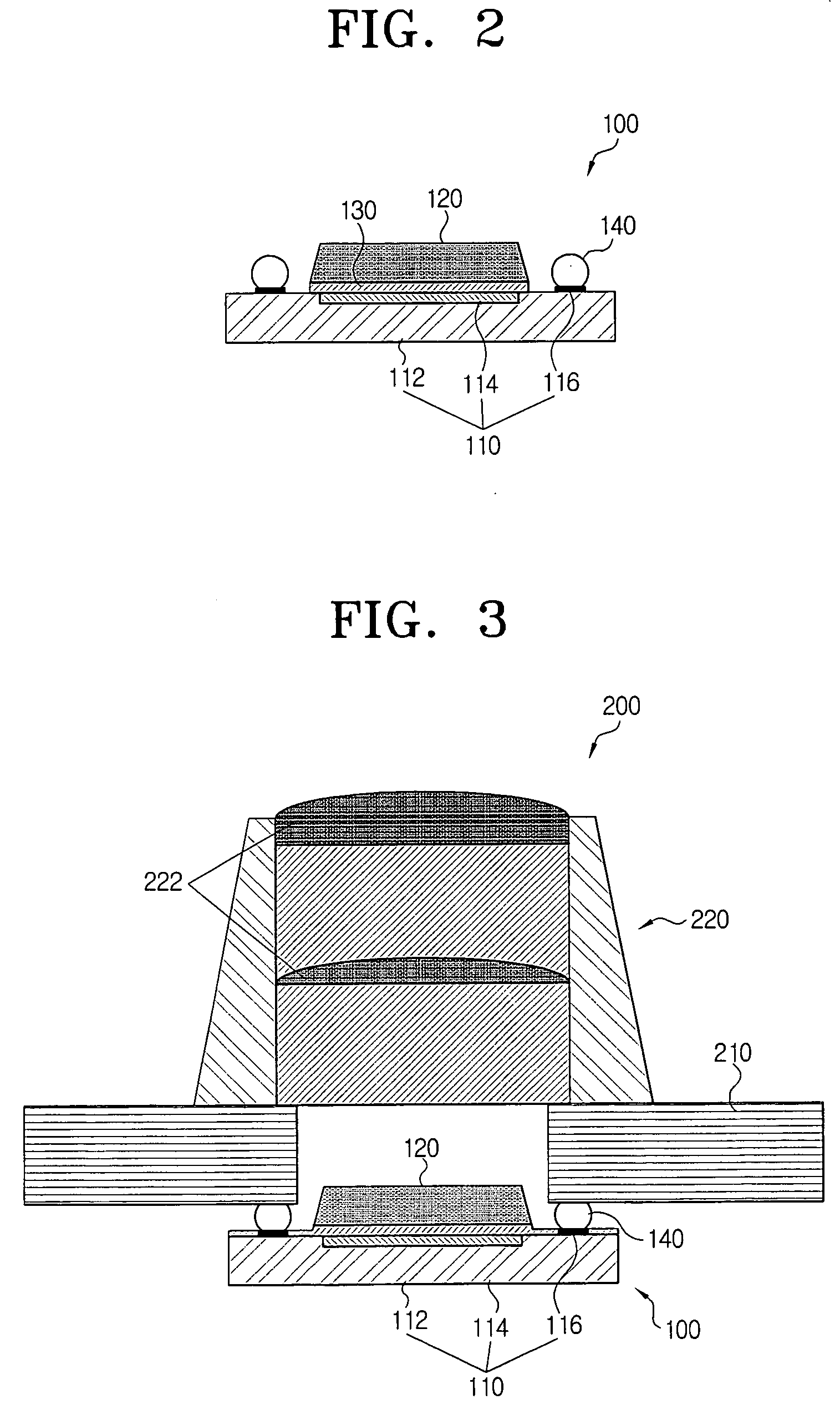
[0029] Referring to FIG. 2, an image sensor package 100 includes an image sensor chip 110, a transparent plate 120, and a connector 140.

[0030] The image sensor chip 110 is provided with an image sensor 114 and a connection pad 116. As for the image sensor 114, a ph...


PUM


Abstract

An image sensor package and a solid state imaging device. The image sensor package includes an image sensor having an image sensor and connection pads on a wafer. A transparent plate is attached to the upper surface of the image sensor chip via an adhesive. The connection pads include connectors, and the image sensor package exchanges signals with a main board of the solid image device through the connectors.

Description

CROSS-REFERENCE TO RELATED APPLICATIONS [0001] This application claims the benefit of Korean Patent Application No. 2004-111255 filed Dec. 23, 2004, in the Korean Intellectual Property Office, the disclosure of which is incorporated herein by reference. BACKGROUND OF THE INVENTION [0002] 1. Field of the Invention [0003] The present invention relates to a semiconductor package; and, more particularly, to an image sensor package, a solid state imaging device, and fabrication methods thereof. [0004] 2. Description of the Related Art [0005] A semiconductor device fabricated on a wafer, e.g., a chip is fragile and therefore, cannot be directly handled by a user as an electric device. Thus, packaging is required to use the semiconductor device as well as to protect the same. The semiconductor device fabricated on a wafer is completed by packaging in a semiconductor package. [0006] An image sensor package is used as a semiconductor package for solid state imaging in applications such as a ...

Claims


Application Information

Patent Timeline
Patent Type & Authority Applications(United States)
IPC IPC(8): H01L31/0203
CPCH01L27/14618H01L27/14625H01L27/14685H01L2224/48227H01L2224/48465H01L2224/73265H01L2924/01079H01L2924/15311H01L2224/32225H01L2924/00H01L23/12H01L23/48H01L23/52H01L27/14
Inventor SHIN, KYU-HOMOON, CHANG-YOULDARBINIAN, ARTHUR
Owner SAMSUNG ELECTRONICS CO LTD
Why Eureka
Try Eureka