Semiconductor device

a technology of semiconductors and devices, applied in the direction of semiconductor devices, electrical equipment, transistors, etc., to achieve the effect of reducing the area of low-voltage transistors, reducing the breakdown voltage level, and chip area

Inactive Publication Date: 2006-06-29
DONGBU ELECTRONICS CO LTD
View PDF7 Cites 15 Cited by
  • Summary
  • Abstract
  • Description
  • Claims
  • Application Information

AI Technical Summary

Benefits of technology

[0011] An advantage of the present invention is to provide a semiconductor device, by which a sufficient breakdown voltage level can be enabled in a high-voltage transistor area, by which on-resistance and leakage current can be enhanced, and by which the chip area in a low-voltage transistor area can be reduced.
[0012] Additional features and advantages of the invention will be set forth in the description which follows and in part will be apparent from the description, or may be learned by practice of the invention. The objectives and other advantages of the invention will be realized and attained by the structure and method particularly pointed out in the written description and claims hereof as well as the appended drawings.
[0013] To achieve these and other advantages and in accordance with the purpose of the invention, as embodied and broadly describ

Problems solved by technology

Yet, in the high-voltage transistor area, it is difficult for the shallow-

Method used


Image

  • Semiconductor device
  • Semiconductor device
  • Semiconductor device

Examples


Embodiment Construction

[0019] Reference will now be made in detail to embodiments of the present invention, examples of which are illustrated in the accompanying drawings. Wherever possible, like reference designations will be used throughout the drawings to refer to the same or similar parts.

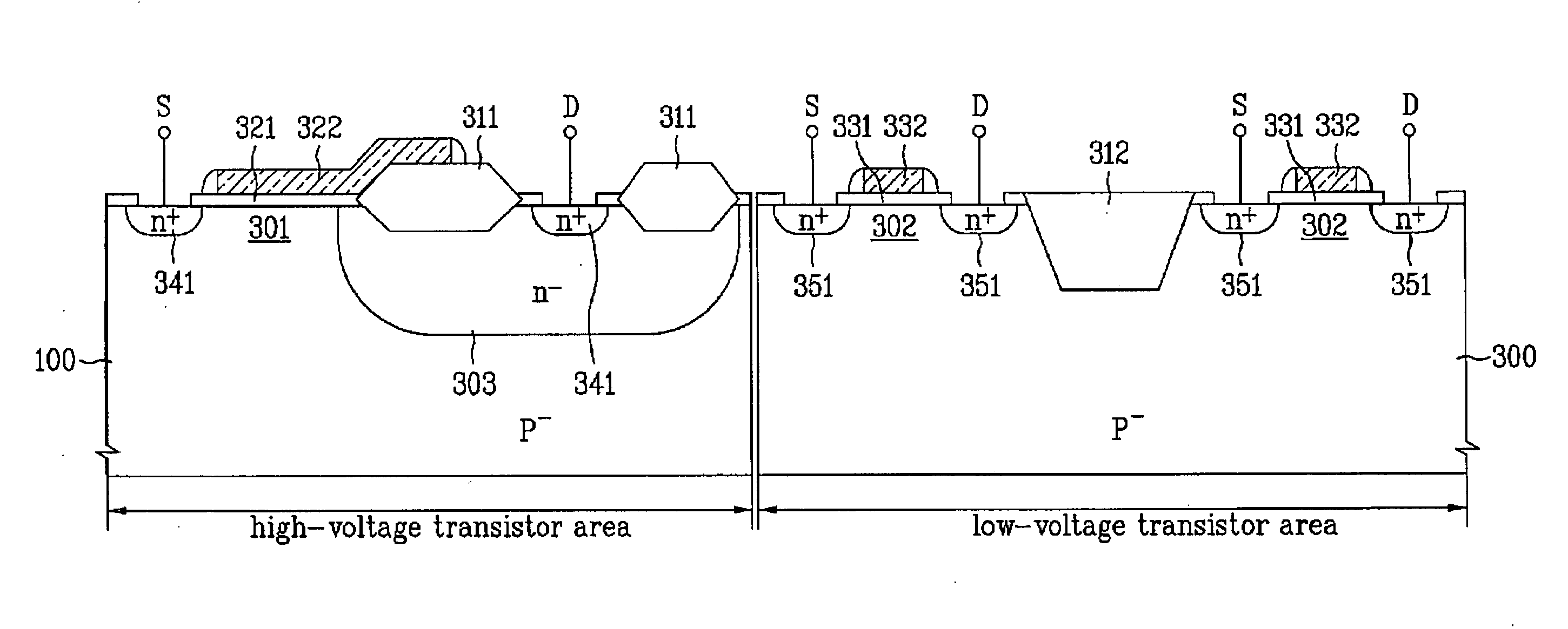
[0020] Referring to FIG. 3, illustrating a semiconductor device according to the present invention, a high-voltage transistor of about 30V or higher is arranged in a high-voltage transistor area and a low-voltage transistor is arranged in a low-voltage transistor area. The low-voltage transistor may be a complementary metal-oxide-semiconductor transistor as used in a logic circuit. A LOCOS layer 311 is used as a device isolation layer in the high-voltage transistor area, whereas a shallow-trench isolation layer 312 is used as a device isolation layer in the low-voltage transistor area. Hence, a breakdown voltage of at least 30V can be obtained in the high-voltage transistor area. Also, the chip area in the low-volta...


PUM


Abstract

A semiconductor device includes a substrate including a high-voltage transistor area provided with a high-voltage transistor and a low-voltage transistor area provided with a low-voltage transistor; a LOCOS layer provided as a device isolation layer of the high-voltage transistor area; and a shallow-trench isolation layer provided as a device isolation layer of the low-voltage transistor area. Accordingly, a sufficient breakdown voltage level can be provided in a high-voltage transistor area, on-resistance and leakage current can be enhanced, and the chip area in a low-voltage transistor area can be reduced.

Description

[0001] This application claims the benefit of Korean Patent Application No. 10-2004-0115645, filed on Dec. 29, 2004, which is hereby incorporated by reference for all purposes as if fully set forth herein. BACKGROUND OF THE INVENTION [0002] 1. Field of the Invention [0003] The present invention relates to a semiconductor device, and more particularly, to a semiconductor device having respective areas for high-voltage and low-voltage transistors. [0004] 2. Discussion of the Related Art [0005] Referring to FIG. 1, illustrating a semiconductor device according to a related art, a high-voltage transistor of about 30V or higher is arranged in a high-voltage transistor area and a low-voltage transistor is arranged in a low-voltage transistor area. A local oxidation of silicon (LOCOS) layer 111 is used as a device isolation layer for each of the high- and low-voltage transistors. [0006] The high-voltage transistor includes n+type source / drain regions 141 provided in predetermined upper par...

Claims


Application Information

Patent Timeline
IPC IPC(8): H01L29/00
CPCH01L21/76202H01L21/76224H01L21/823462H01L21/823481H01L27/088H01L29/0653H01L29/42368H01L29/7835H01L21/18
Inventor KO, KWANG YOUNG
Owner DONGBU ELECTRONICS CO LTD
Why Eureka
Try Eureka