Semiconductor device with a high breakdown voltage,low on-resistance,lateral power mosfet

a technology of lateral power mosfet and semiconductor device, which is applied in the direction of semiconductor device, transistor, electrical apparatus, etc., can solve the problems of device liable to cause a reduction in electron mobility, and the on-resistance of the transistor to ris

Inactive Publication Date: 2001-01-23
TOYOTA CENT RES & DEV LAB INC
View PDF6 Cites 68 Cited by
  • Summary
  • Abstract
  • Description
  • Claims
  • Application Information

AI Technical Summary

Benefits of technology

In the above described semiconductor device, insulation layers are formed at the two sides of a drain region (the fourth semiconductor layer) and the drain region is formed into a deeper region than the insulation layer. By having the drain region come into contact with the drain drift region (the first semiconductor layer) at a portion beneath the insulation layer, the drift length can be shortened while ensuring a sufficient level of breakdown voltage.
In other words, by providing an insulation layer at a portion of the boundary between the drain region and the drain drift region (from the top of the first semiconductor layer extending to a required depth), the electric field applied to the drain-source regions is distributed with a high degree of uniformity within the above-mentioned insulation layer. Since the above structure is less prone to uneven electric field distribution, this allows a greater breakdown voltage for the device.

Problems solved by technology

This has presented a disadvantage of a steep rise in on-resistance of a transistor through the increased resistive component of a drain drift region 4.
This leads to an increase in the residual crystal defects or crowding of the current flow paths within the diffusion layer which forms a channel, thereby making the device liable to cause a reduction in electron mobility.

Method used


Image

  • Semiconductor device with a high breakdown voltage,low on-resistance,lateral power mosfet
  • Semiconductor device with a high breakdown voltage,low on-resistance,lateral power mosfet
  • Semiconductor device with a high breakdown voltage,low on-resistance,lateral power mosfet

Examples


third embodiment

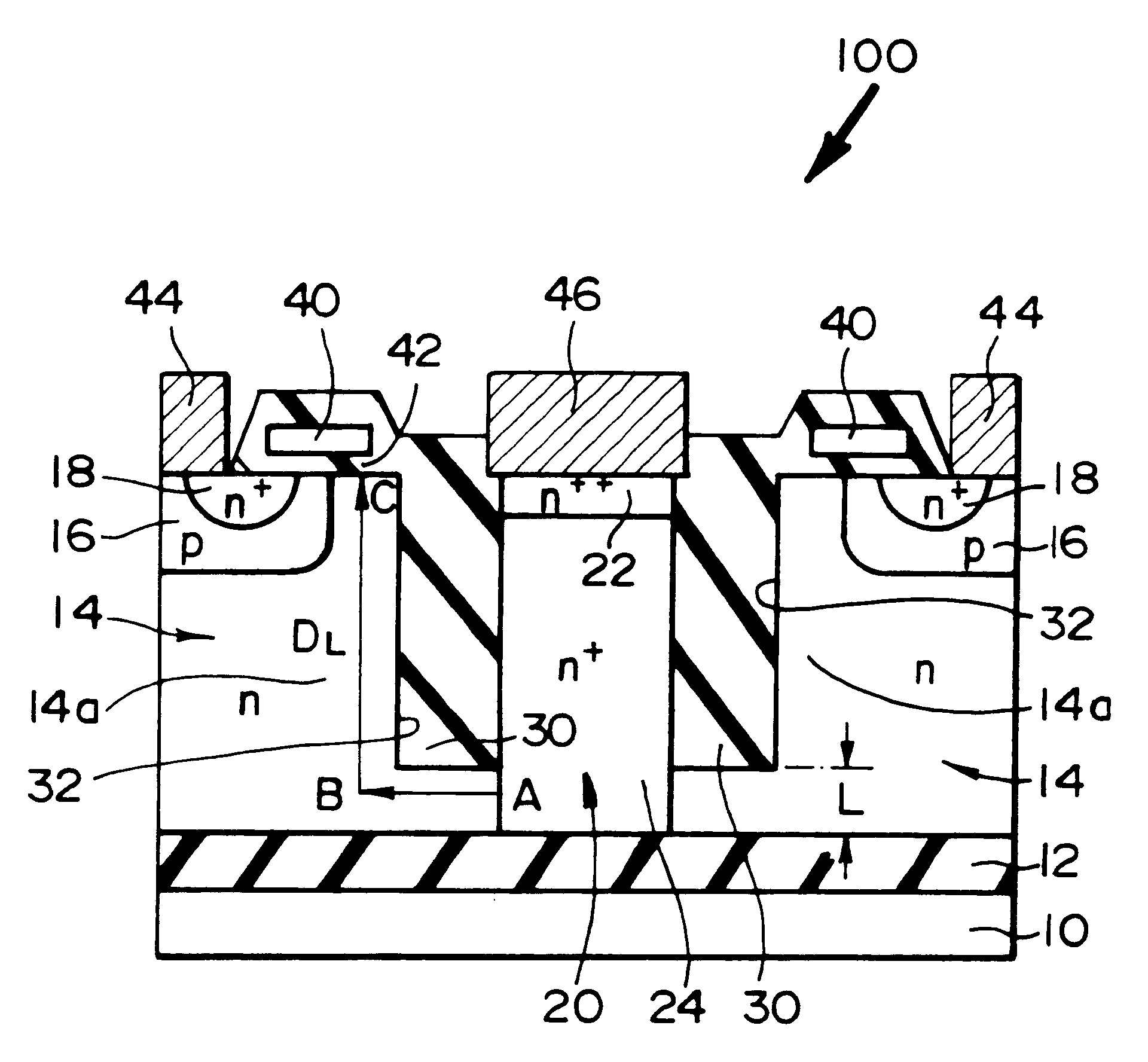
FIG. 9 is a cross-sectional view schematically illustrating an example of a semiconductor device wherein the present invention is applied to a lateral power MOSFET configured with a trench gate structure. The semiconductor device of the present embodiment is similar to the aforementioned second embodiment except it has an SOI structure. Constituent parts providing functions essentially identical to those used in the semiconductor of the second embodiment will be indicated with the same symbols.

The semiconductor device 300 shown in FIG. 9 comprises a silicon substrate 10, an insulating substrate 12, and a first semiconductor layer 14 doped with an n-type impurity and formed on the insulating substrate 12 to constitute a drain drift region 14a. Description with regard to the SOI structure is omitted here as it has been dealt with in the first embodiment.

On the upper main surface of the first semiconductor layer 14 there is located a p-type body region 16 (the second semiconductor laye...

fourth embodiment

FIG. 10 is a cross-sectional view schematically illustrating an example of a semiconductor device wherein the present invention is applied to a lateral power MOSFET configured with a trench gate structure. The semiconductor device of the present embodiment is similar to the aforementioned second embodiment with exception that it has an SOI structure and a different system for trench isolation. Constituent parts providing functions essentially identical to those used in the semiconductor of the second embodiment will be indicated with the same symbols.

The semiconductor device 400 shown in FIG. 10 comprises a silicon substrate 10, an insulating substrate 12, and a first semiconductor layer 14 doped with an n-type impurity and formed on the insulating substrate 12 to constitute a drain drift region 14a. Description with regard to the SOI structure is omitted here as it has been dealt with in the first embodiment.

On the upper main surface of aforementioned first semiconductor layer 14 t...

fifth embodiment

FIG. 11 is a cross-sectional view schematically illustrating an example of a semiconductor device wherein the present invention is applied to a lateral power MOSFET configured with a trench gate structure. The semiconductor device of the present embodiment is structured similarly to the aforementioned second embodiment with exception that it is based on an SOI structure and a different configuration for the drain electrode. Constituent parts providing functions essentially identical to those used in the semiconductor of the second embodiment will be indicated with the same symbols.

The semiconductor device 500 shown in FIG. 11 comprises a silicon substrate 10, an insulating substrate 12, and a first semiconductor layer 14 doped with an n-type impurity and formed on the insulating substrate 12 to constitute a drain drift region 14a. Description with regard to the SOI structure is omitted here as it has been dealt with in the first embodiment.

On the upper main surface of aforementioned...


PUM


Abstract

A semiconductor device containing a lateral MOS transistor comprising a silicon substrate, an n-type first semiconductor layer constituting a drain drift region, a p-type second semiconductor layer prepared within the first semiconductor layer to constitute a body region and with a channel region formed within a portion of said body region, an n-type third semiconductor layer prepared on the surface of the second semiconductor layer to constitute a source region, an n-type fourth semiconductor layer constituting a drain region, and an insulation layer that is constituted of insulating material filled into a trench prepared in the first semiconductor layer and arranged along the two sides of the drain region. The drain region is formed into a region deeper than the insulation layer and in contact with the drain drift region at a portion beneath the insulation layer. The semiconductor device provides a high breakdown voltage and a low on-resistance, and can be fabricated with a reduced cell pitch.

Description

1. Field of the InventionThe present invention relates to a semiconductor device containing a lateral MOS transistor. More specifically, the present invention relates to technology suitable for use in a high breakdown voltage, low on-resistance, lateral power MOSFET that can be microminiaturized.2. Description of the Related ArtA high breakdown voltage lateral trench MOSFET disclosed in the Japanese Patent Application Laid-Open No. 8-97411 has, as shown in FIG. 12, a p-type well region 2 formed on a p-type substrate 1, a diffusion layer comprising a source region 9 and a body region 8 formed within the above well region 2 using a double diffusion process with a self alignment technique, and a gate oxide layer 6 and a gate electrode 7 located on top of the structure. Further, a trench 3 is formed by a trench work within a drain drift region 4 to secure the drift length for accomplishing a high breakdown voltage. In the above-described structure, when a gate voltage is applied, electr...

Claims


Application Information

Patent Timeline
Patent Type & Authority Patents(United States)
IPC IPC(8): H01L29/66H01L29/06H01L27/12H01L29/78H01L29/02H01L21/336H01L29/786
CPCH01L27/1203H01L29/0653H01L29/7809H01L29/7812H01L29/7813H01L29/7824H01L29/41766
Inventor SUZUKIKAWAJI, SACHIKOUESUGI, TSUTOMU
Owner TOYOTA CENT RES & DEV LAB INC
Why Eureka
Try Eureka