Vertical alignment liquid crystal display device

a liquid crystal display and active matrix technology, applied in optics, non-linear optics, instruments, etc., can solve the problems of low aperture ratio and uneven display, and achieve the effect of stable alignmen

Inactive Publication Date: 2006-06-29
CASIO COMPUTER CO LTD
View PDF67 Cites 27 Cited by
  • Summary
  • Abstract
  • Description
  • Claims
  • Application Information

AI Technical Summary

Benefits of technology

[0052] According to the liquid crystal display device of the third aspect of the invention, the lying directions of the liquid crystal molecules in each pixel are defined by the rubbing directions of the vertical alignment films and by a liquid crystal molecule alignment direction near the V-shaped edge of the pixel electrode when a voltage is applied between the pixel electrodes and the opposing electrode, enabling the liquid crystal display device to obtain a stable state of al...

Problems solved by technology

Such a vertical alignment liquid crystal display device causes variation in the state of lying alignment of the liquid crystal molecules in accordance with the voltages applied to the respective pixels, resulting in display unev...

Method used


Image

  • Vertical alignment liquid crystal display device
  • Vertical alignment liquid crystal display device
  • Vertical alignment liquid crystal display device

Examples


first embodiment

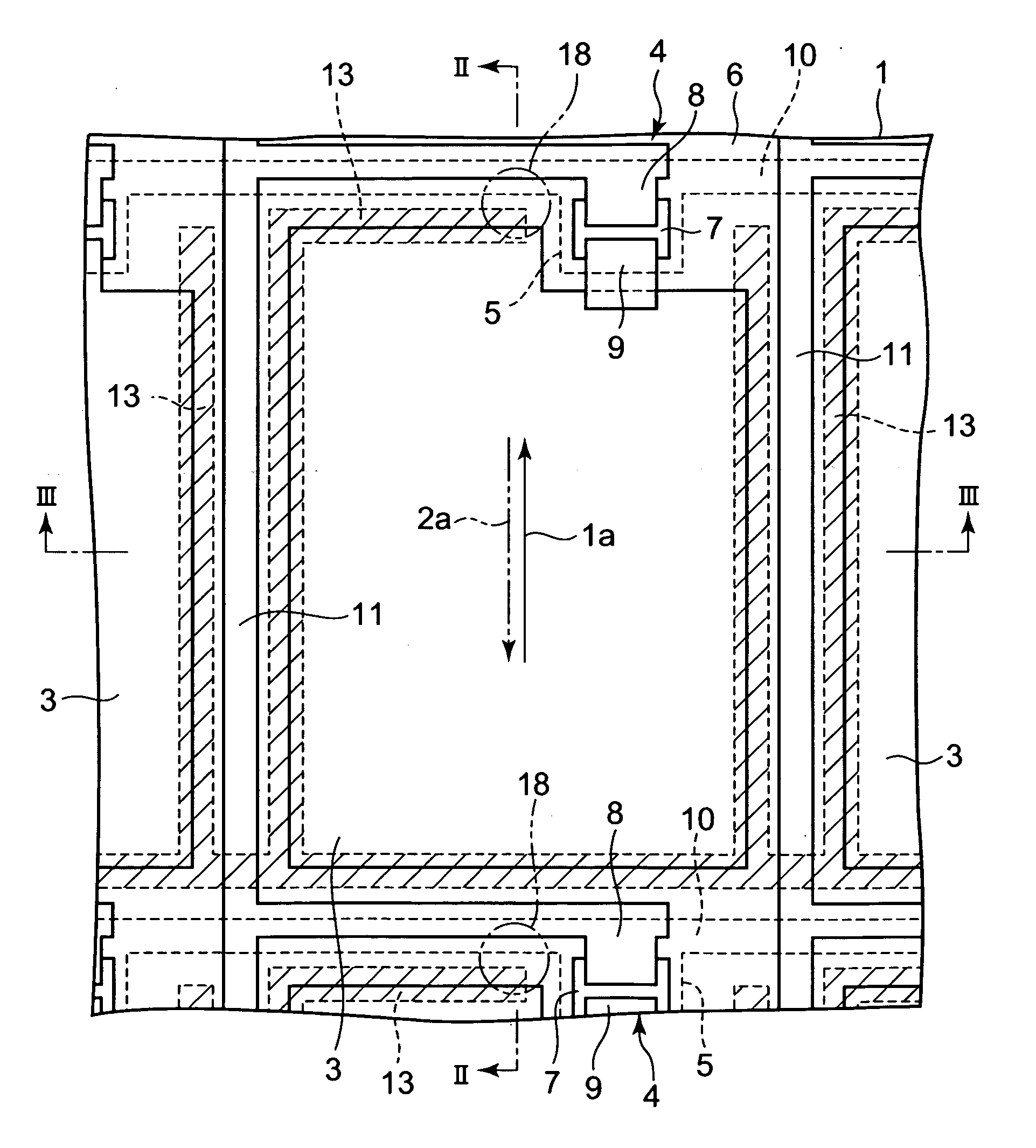
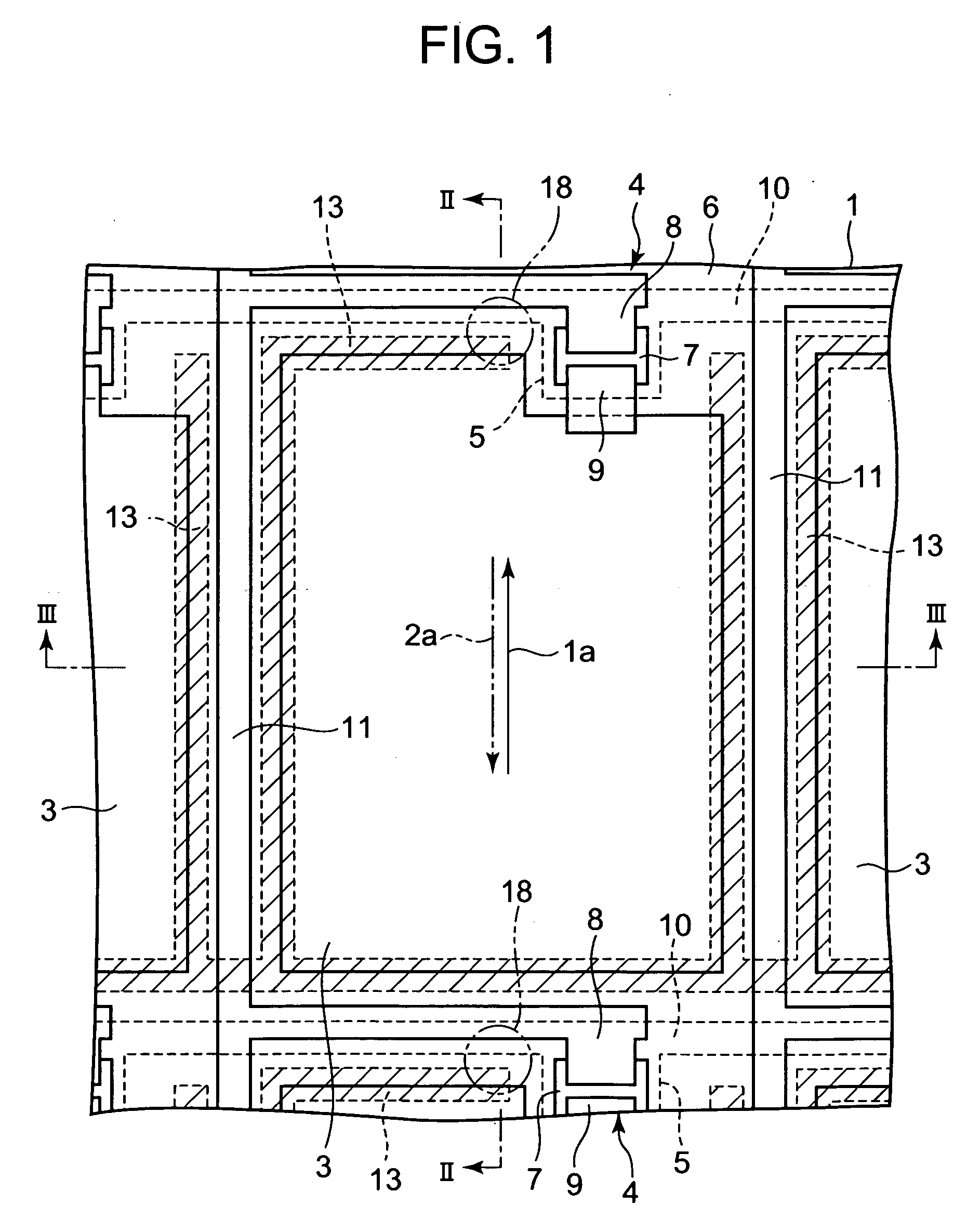
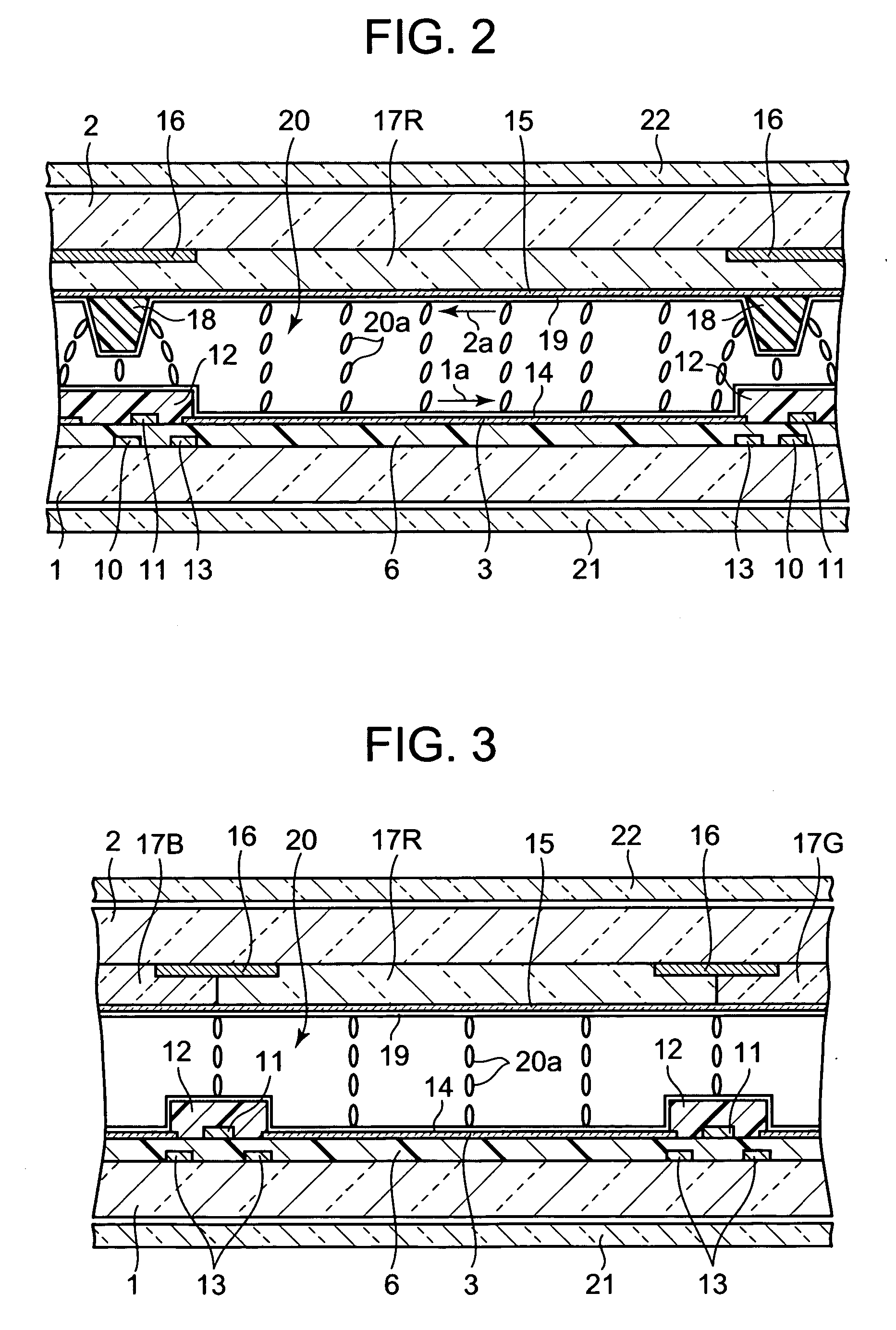
[0066]FIG. 1 to FIG. 5 show the first embodiment of the present invention, where FIG. 1 is a plan view of one pixel on one substrate of a liquid crystal display device, and FIG. 2 and FIG. 3 are cross sections of the liquid crystal display device of FIG. 1, as cut along the line II-II and the line III-III respectively.

[0067] The liquid crystal display device is a vertical alignment active matrix liquid crystal display device, and comprises a pair of transparent substrates 1 and 2 opposite to each other with a predetermined gap therebetween as shown in FIG. 1 to FIG. 3. At least one transparent opposing electrode 15 is formed on the inner surface of one substrate of the opposing inner surfaces of the pair of substrates 1 and 2, for example, on the inner surface of the substrate 2 on the viewer side (hereinafter referred to as front substrate). Formed on the inner surface of the other substrate of the opposing inner surfaces of the pair of substrates 1 and 2, i.e., on the inner surfa...

second embodiment

[0101]FIG. 6 is a cross sectional view of one pixel of a liquid crystal display device as the second embodiment of the present invention. In the present embodiment, the components same as those in the first embodiment will be given the same reference numerals, and explanation for such components will be omitted.

[0102] The liquid crystal display device according to the present embodiment has a plurality of protrusions 118 on the inner surface of the front substrate 2 formed to have a predetermined height of protrusion for setting the thickness of the liquid crystal layer to a predetermined one, and has the end of the plurality of protrusions 118 abut on the inner surface of the rear substrate 1 (abut on the overcoat insulation film 12 between the plurality of pixel electrodes 3), thereby defining the gap between the pair of substrates 1 and 2. The structure of the liquid crystal display device of the present invention is the same as that of the liquid crystal display device of the f...

third embodiment

[0104]FIG. 7 is a plan view of one pixel on one substrate of a liquid crystal display device as the third embodiment of the present invention. In the present embodiment, the components same as those in the first embodiment will be given the same reference numerals, and explanation for such components will be omitted.

[0105] The liquid crystal display device according to the present embodiment is not provided with the plurality of protrusions 18 that are provided on the inner surface of the front substrate 2 according to the first embodiment, but has the thin film transistors (TFTs) function as the protrusions 18 in order to stabilize the state of alignment of the liquid crystal molecules by the gate field of the TFTs and the electric field generated between the pixel electrodes 3. Hence, the present liquid crystal display device has each of a plurality of TFTs 41 on the inner surface of the rear substrate 1 positioned at about the center of one edge of each of the pixel electrodes 3...


PUM

PropertyMeasurementUnit
Fractionaaaaaaaaaa
Angleaaaaaaaaaa
Angleaaaaaaaaaa

Abstract

A liquid crystal display device has rear and front substrates having pixel electrodes and an opposing electrode formed on their opposing inner surfaces respectively, vertical alignment films formed on their opposing inner surfaces respectively, and a liquid crystal layer disposed between the vertical alignment films and having negative dielectric anisotropy. Protrusions are formed on the inner surface of the front substrate, at a position adjoining one edge of each of the pixel electrodes formed on the inner surface of the rear substrate, correspondingly to a position about the center of the one edge of the pixel electrode. The vertical alignment film on the inner surface of the rear substrate is rubbed in a direction from an edge opposite to the one edge of the pixel electrode adjoining the protrusion toward the one edge. The vertical alignment film on the inner surface of the front substrate is rubbed in reverse direction.

Description

BACKGROUND OF THE INVENTION [0001] 1. Field of the Invention [0002] The present invention relates to a vertical alignment active matrix liquid crystal display device using a thin film transistor (hereinafter referred to as TFT) as an active element. [0003] 2. Description of the Related Art [0004] A vertical alignment liquid crystal display device comprises a pair of substrates opposite to each other with a predetermined gap therebetween, a plurality of pixel electrodes arranged in a matrix of rows and columns on the inner surface of one substrate of the opposing inner surfaces of the pair of substrate, a plurality of TFTs arranged on the inner surface of the one substrate correspondingly to the plurality of pixel electrodes and connected to the corresponding pixel electrodes, a plurality of gate lines and data lines formed on the inner surface of the one substrate respectively between the rows of pixel electrodes and the columns of pixel electrodes for supplying a gate signal and a ...

Claims


Application Information

Patent Timeline
IPC IPC(8): G02F1/1337
CPCG02F1/133707G02F1/133711G02F1/13394G02F2001/133742G02F1/133742
Inventor ANDO, SHINYANAKAJIMA, YASUSHI
Owner CASIO COMPUTER CO LTD
Why Eureka
Try Eureka