

Probe device and probe method
a probe device and probe technology, applied in the field of probe devices, can solve the problems of reduced inspection reliability, excessive contact load, failure to obtain the desired contact load, etc., and achieve the effect of rapid revising load, constant contact load, and highly reliable inspection
- Summary
- Abstract
- Description
- Claims
- Application Information
AI Technical Summary
Benefits of technology
Problems solved by technology
Method used
Image


Examples
Embodiment Construction
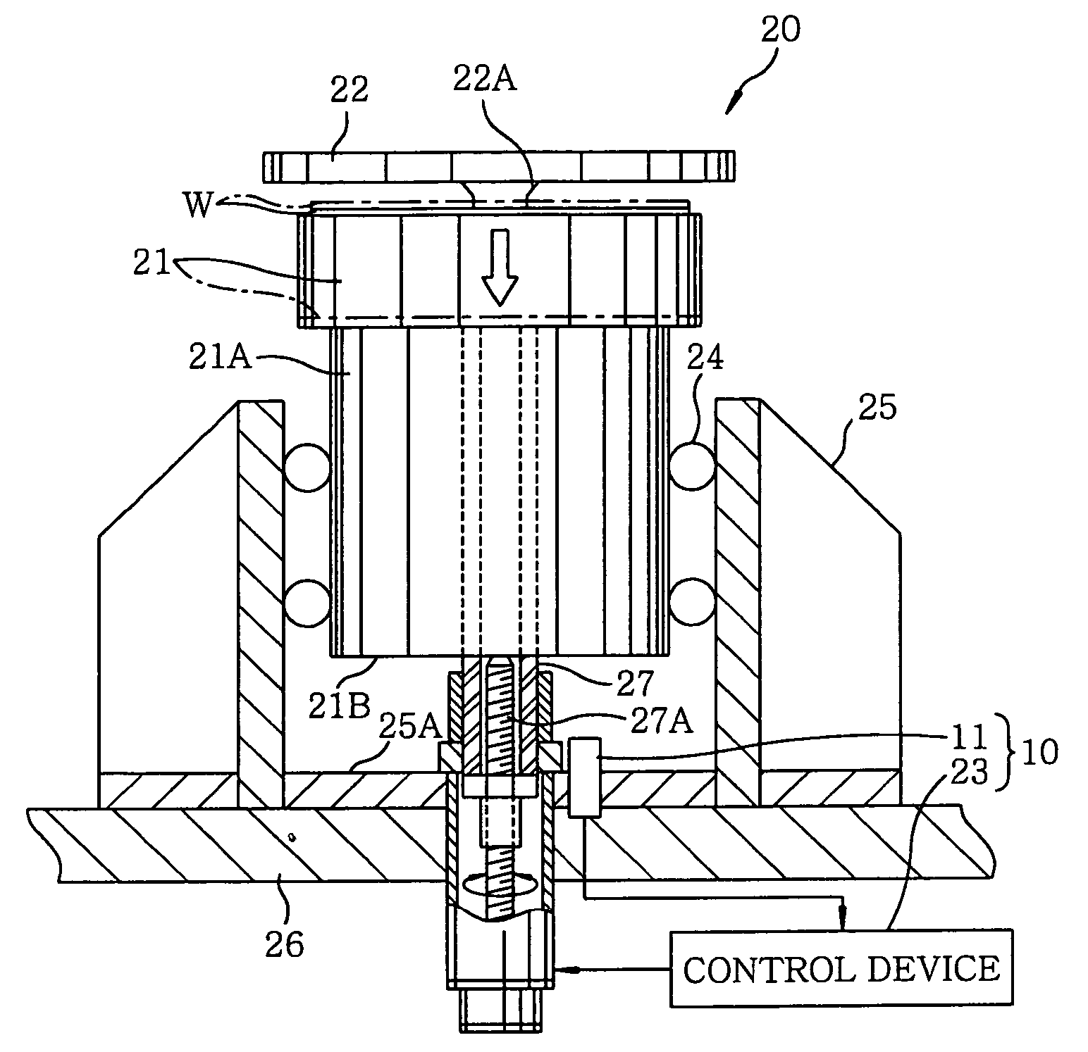
[0021] The present invention will now be described with reference to an embodiment shown in FIG. 1. As shown in FIG. 1, a probe device 20 of the present embodiment is provided with a contact load monitoring device 10 for monitoring a contact load exerted by a probe card 22 during inspection.
[0022] The probe device 20 of the preferred embodiment will now be described. As shown in FIG. 1, the probe device 20 of the present invention may include, for example, an XY stage 26; a linear driving mechanism 27; a main chuck 21 capable of moving in X, Y, Z and θ directions while carrying a wafer W mounted thereon; the probe card 22 disposed above the main chuck 21 and provided with a plurality of probes 8A; and an alignment mechanism 7 (see FIG. 2A) to determine the position of the wafer W mounted on the main chuck 21. Under the control of a control device 23, the aligned main chuck 21 is elevated, so that the wafer W is brought into contact with the probes 22A. Electrical characteristics of...
PUM
 Abstract
Description
Claims
Application Information